
Light-electron interaction
In the classical model, nuclei and electrons can be described by a spring system.
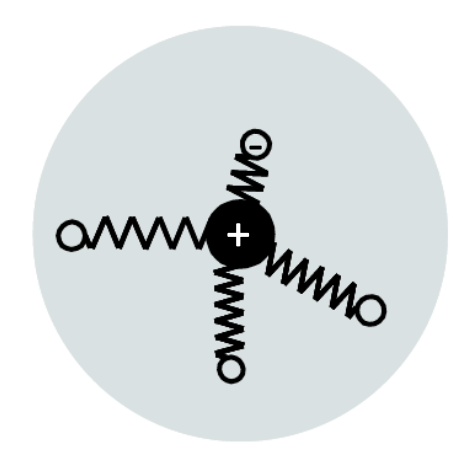
The electrons are held in a stable orbit with respect to the heavy nucleus by springs which represent the restoring forces due to the binding between them. The negatively charged electron and the positively charged nucleus form an electric dipole with a magnitude proportional to their separation.
Light is characterized by a harmonically oscillating magnetic and electric field.
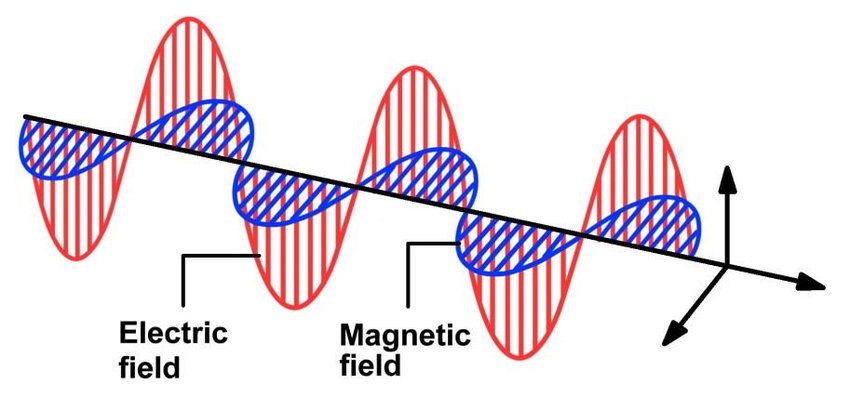
If we shine a light on an atom, the photons electric field exerts a force on electrons and nucleus and drives oscillations of the system at frequency
If
The absorption strength is characterized by the absorption coefficient
To describe the optical transitions and the overall absorption coefficient in materials we rely on the Fermi’s golden rule which estimates the probability per unit of time that a quantum system will transition from an initial state
The rate is influenced by mainly two factors.
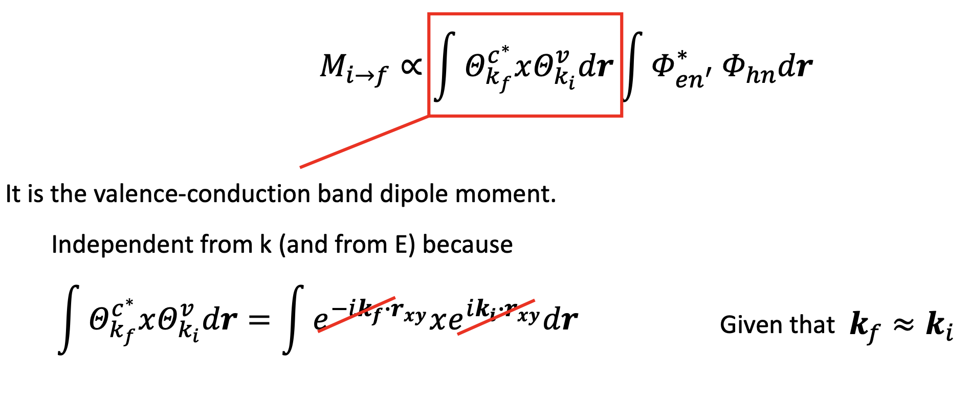
The matrix element
Where
The physical meaning of
The square of the absolute value of the matrix element,
The delta function:
This part ensures that energy is conserved during the transition. The transition can only occur if the energy of the photon (
Joint density of states
In semiconductors, light absorption creates energetic electrons and electron vacancies or holes. The optical absorption is given by the rate of all possible transitions allowed by a given photon energy
where
In the limit of a large system (where
now we can write the joint density of states as:
The image below show a band structure where the blue arrows represent electron transitions due to photon absorption:
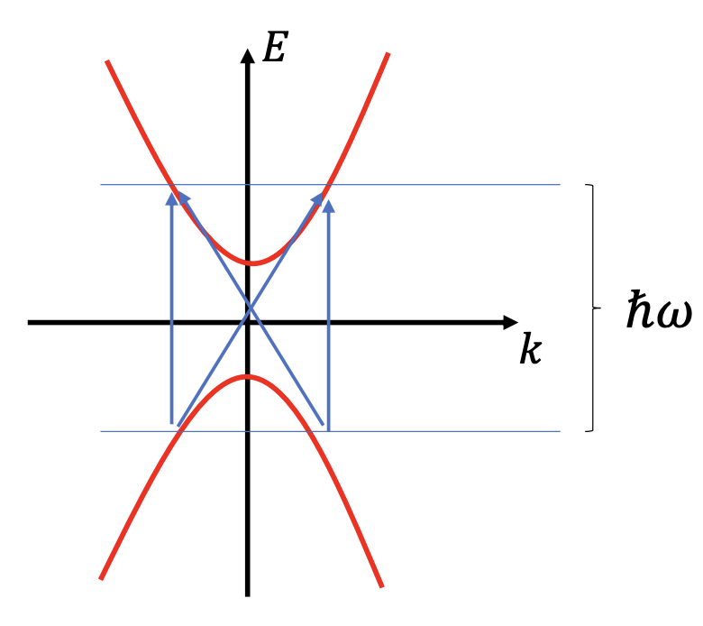
in addition to the conservation of energy we must also satisfy the momentum conservation:
where
The wavelength of the incident radiation (infrared region, visible, up to near and far ultraviolet region) is much larger than the lattice parameter; in these situations, the photon wavevector
This is why vertical transitions are the most likely.
Excitons
The absorption process in a semiconductor or insulator creates an electron in the conduction band and a hole in the valence band but we have previously neglected the Coulomb attraction between them: this can give rise to the formation of new excitations called exciton. An exciton is a quasiparticle, it’s formed when an electron absorbs enough energy to jump to a higher energy level, leaving behind a hole. The opposite charge particles are created at the same point in space and can attract each other and form a bound electron-hole pair which is called exciton.
In the simplest picture the exciton may be conceived as a small hydrogenic system.
There are two basic types of excitons:
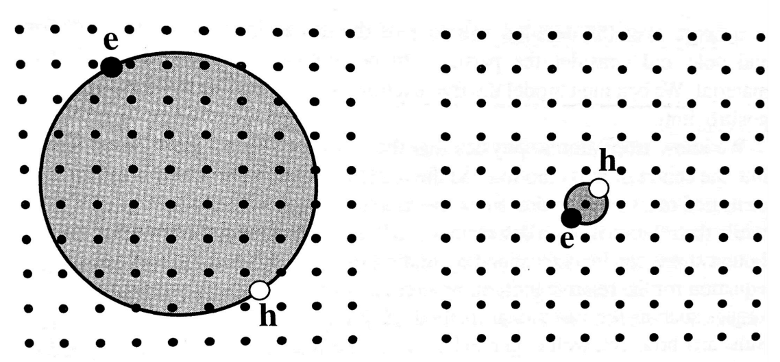
Wannier-Mott excitons (or free excitons)
They are delocalized states that can move freely throughout the crystal
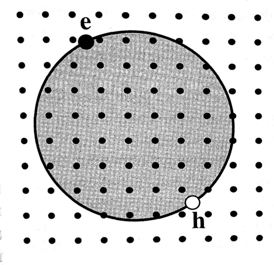
A free exciton can be modelled as a hydrogenic system, the energy of the bound states can be obtained by finding the eigenvalues of the Schrödinger equation for an electron moving in the field generated by a positive charge.
Solving the Schrödinger equation we get that:
where
We also need to know that
Free excitons are commonly found in semiconductors with direct band gaps, like
The group velocity for an electron or hole within a band can be calculated using the following equation:
At the zone center, bands have a flat or zero gradient. Consequently, when there’s a direct transition occurring at
The energy of the exciton created in a direct transition at
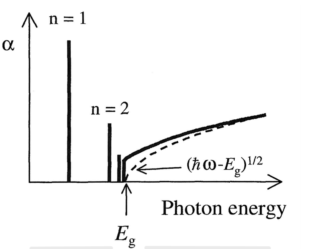
Band edge absorption spectrum for a direct gap semiconductor with excitonic effects.
The dashed line shows the expected absorption when the excitonic effects are ignored. When excitons form, they create distinct absorption peaks in the material’s optical absorption spectrum. These peaks occur at energies slightly lower than the bandgap energy of the material. The presence of these exciton peaks increases the absorption coefficient at specific energies.
Free exciton absorption can only be observed in the absorption spectrum of very pure samples. This is because impurities releases free electrons ad holes that can screen the Coulomb interaction in the exciton and thereby strongly reduce the binding forces. Excitonic effects are not usually observed in doped semiconductors or metals, since they contain a very high density of free carriers.
Wannier-Mott excitons have small binding energies due to their large radius, with typical values of
Frenkel excitons (or tightly bound excitons)
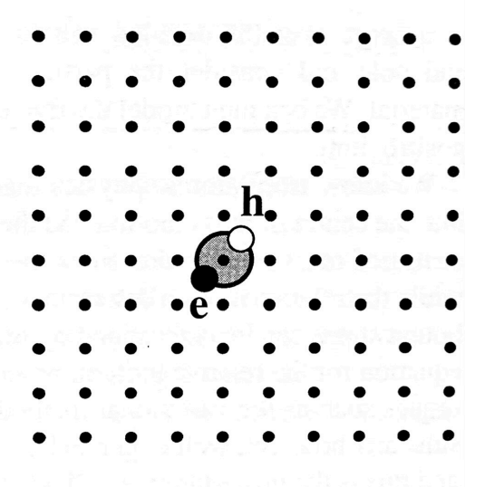
Frenkel exciton occurs in large band gap materials with small dielectric constant and large effective masses and they are localized on the atom site they are generated. They can be considered as excited states of the individual atoms or molecules on which they are localized. They have small radii and correspondingly large binding energies, with typical values ranging from about
Stable excitons will only be formed if the attractive potential is sufficient to protect the exciton against thermal vibrations (phonons). Indeed these effects become stronger as the band gap increases and the temperature is lowered.
Since the maximum energy of a thermally excited phonon at room temperature
QW structures
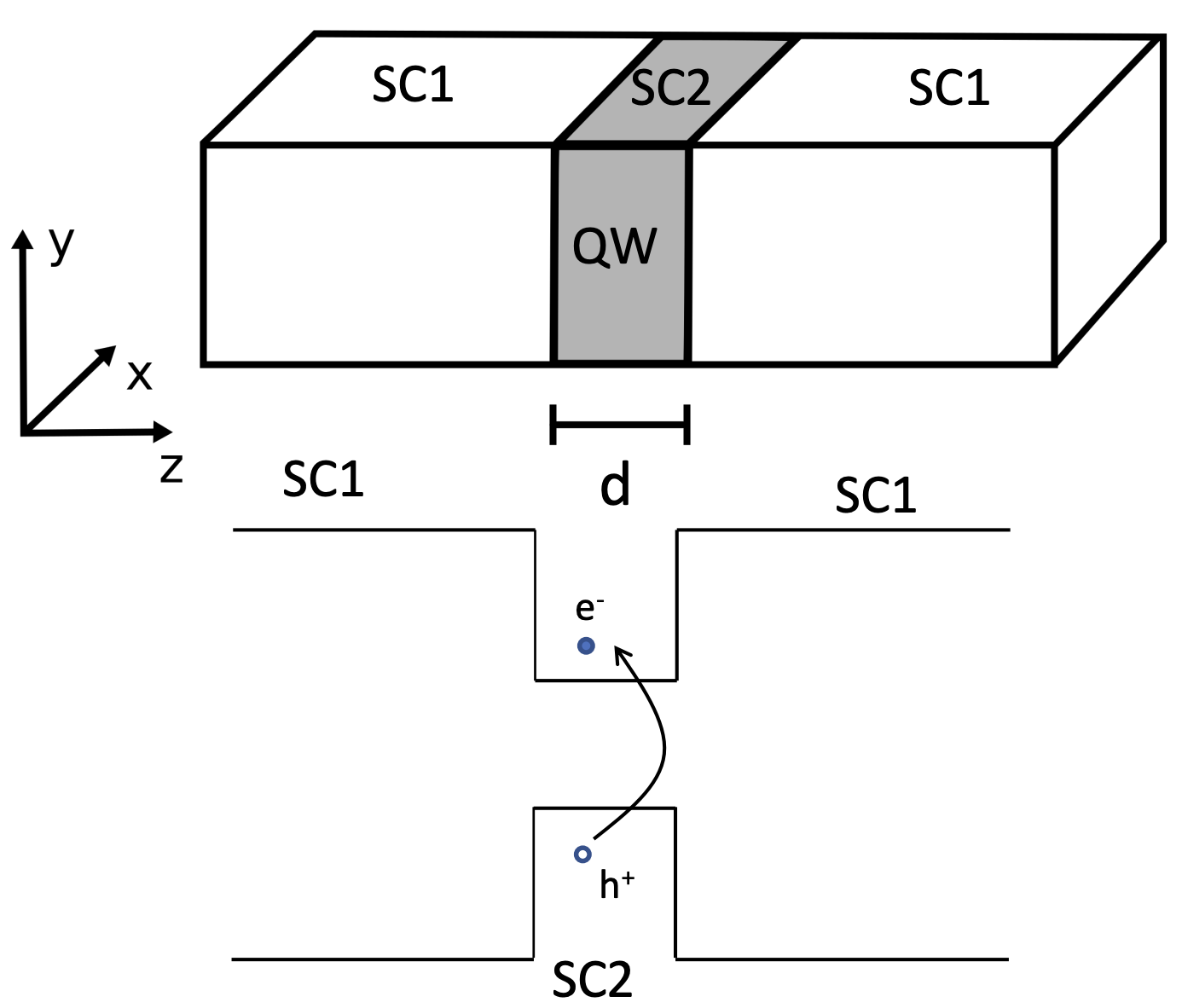
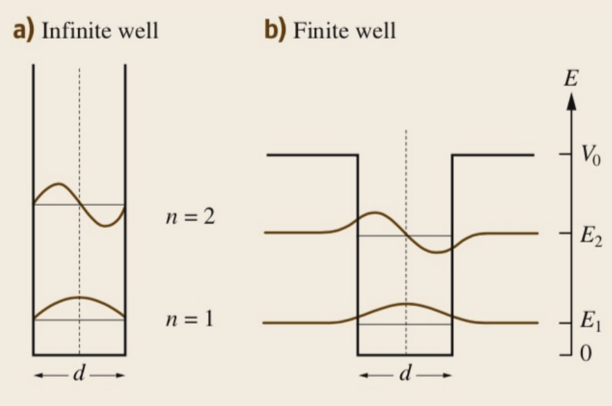
We can calculate the electronic states of QWs by solving the Schrödinger equation for the electrons and holes in the potential wells created by the band discontinuities.
Along the
with
Along the
The total energy for an electron or hole in the quantum level is therefore given by:
The confinement energy is inversely proportional to
The quantization of the motion in the
-
The quantization energy shifts the effective band edge to higher energy. Indeed the quantized energy levels are higher in energy than the unconfined states in the bulk material.
-
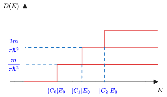
The density of states becomes a stepwise function, whereas the density of states of in a 3D material is proportional to
. 
-
The confinement keeps the electron and holes closer together and hence increases the radiative recombination (the process where an electron in a higher energy state loses energy by emitting a photon and falls into a lower energy state) probability. In a quantum well, the motion of electrons and holes is restricted in the direction perpendicular to the well. This means they are more likely to be found in closer proximity to each other than in a bulk semiconductor where they could be more spread out.
Transitions in QW:
Let’s analyse the transitions between occupied and unoccupied states in a QW:
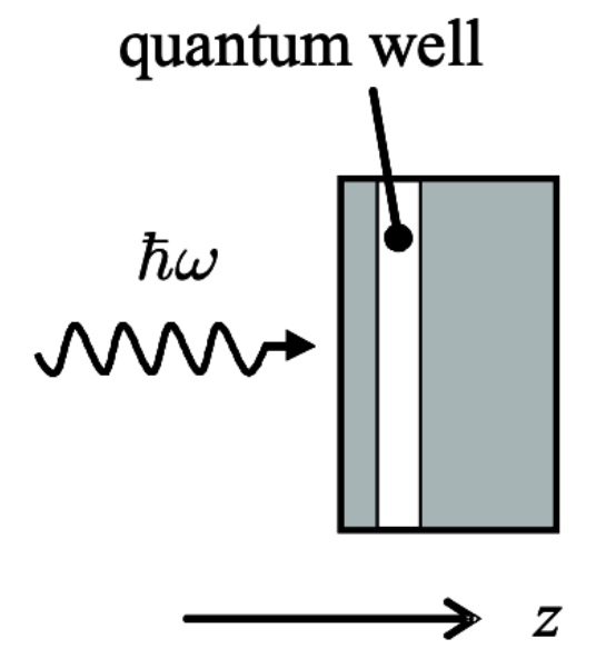
In the typical experiment, light is directed along the
Let us assume the electric field is along x only (the more general result is just a rotation):
Putting all together (forgetting about all the constants):
and
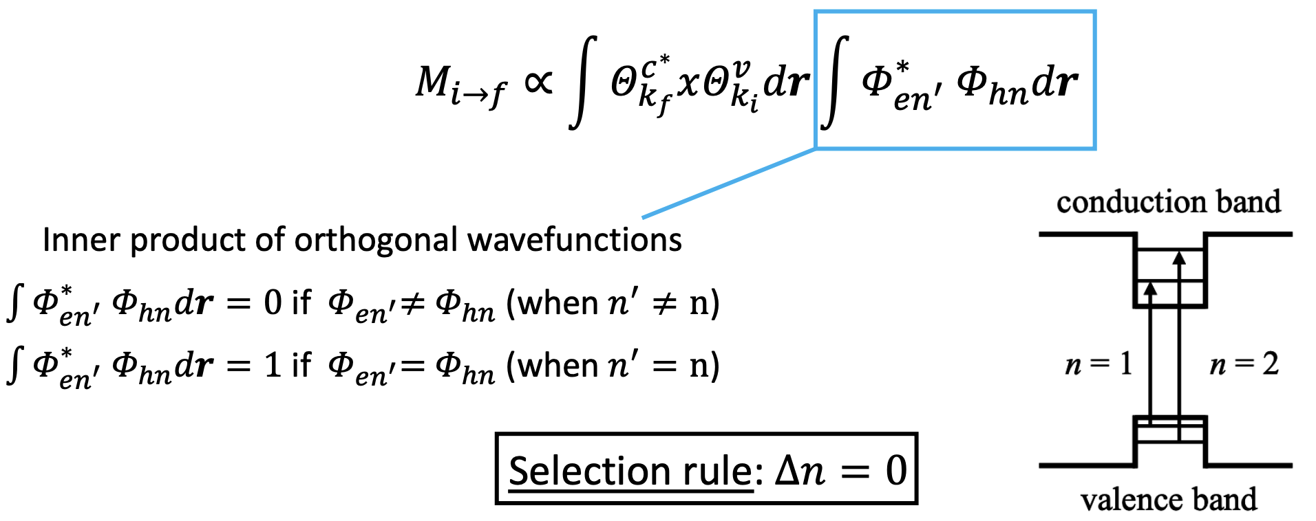
The J is obtained by counting all the initial occupied states and all the unoccupied final states:
we simplified the formulas due to the fact that
The J is calculated with a similar procedure to the regular density of states for a QW. We, therefore, find the same step-like function independent from
where
The result of the DOS is same as the regular density of states for a 2D material.
Just like the regular DOS, the lowest available state (transition) is not given by the band gap, but there is an additional shift. Indeed in a quantum well, the lowest energy level for electrons is not at the bottom of the conduction band as it would be in bulk material. Instead, it is shifted higher due to the confinement effects
The absorption coefficient is directly proportional to the joint density of state and the matrix element:
The transition from a 3-D material to a 2-D QW alters the shape of the absorption curve (stepwise increase of absorption with the frequency), and also causes an effective shift in the bandgap by (
In a quantum well the absorption threshold (the minimum photon energy for absorption to occur) is different from that of the bulk material. Once photons have enough energy to exceed this threshold, they can be absorbed by the electrons, promoting them to the conduction band and leaving behind holes in the valence band. For energies just above the threshold, the absorption coefficient in a QW is constant until you reach the next subband.
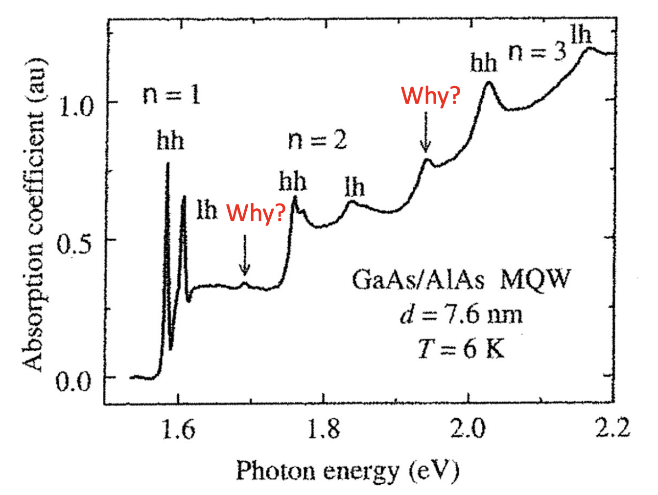
In addition to the ground state transition (from the first electron subband to the first hole subband) we also have excited state transitions. These transitions occur at higher frequencies. The threshold energy for these higher transitions accounts not only for the base band gap of the material but also for the additional energy required to reach the higher quantized electron and hole levels in the quantum well:
Once again we have ignored so far the Coulomb interaction between the electrons and holes that are involved in the transition.
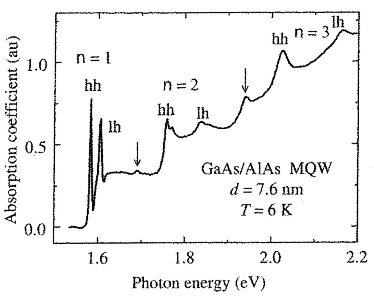
also in this case, the exciton energy lead to sharp lines that occur at:
where
Beyond the selection rule
When calculating the matrix element, it was assumed that we were dealing with solutions of the infinite well.
However, if we consider a more realistic model, a finite well, in the conduction and valence band the wavefunctions will penetrate past the walls differently depending on their effective mass. The conduction and valence states, in this case, are no longer completely orthogonal and there is a small chance to violate the selection rule
The development of quantum wells is driven largely by their application in light-emitting devices, where they offer several distinct benefits over traditional bulk materials:
-
The shift of the luminescence peak by the confinement energy allows the wavelength of the light emitting devices to be tunes by choice of the well width
-
The increase overlap between the electron and hole wavefunctions in the quantum well means that the emission probability is higher.
A simple semiconductor laser diode is made up of the following parts in order:
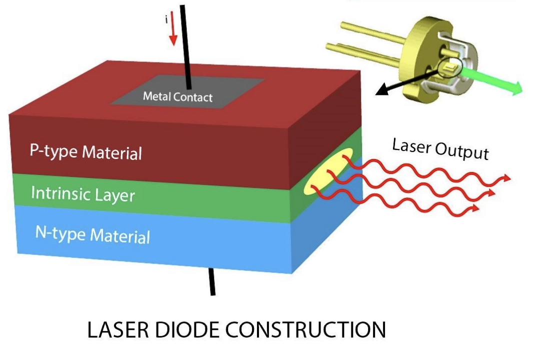
The input terminals of a homojunction laser diode are attached to metal plates, which are in turn bonded to the n-type and p-type semiconductor layers. In this diode, an intrinsic layer is positioned between the p-type and n-type materials. This layer expands the active region’s volume, allowing a larger number of electrons and holes to gather at the junction. As a result, more electrons can recombine with holes at any given time, enhancing the laser’s output power. The laser light is produced from an elliptical area and can be focused using an optical lens. The whole structure, consisting of p-type, intrinsic, and n-type layers (PIN diode), is typically housed in a metal casing.