
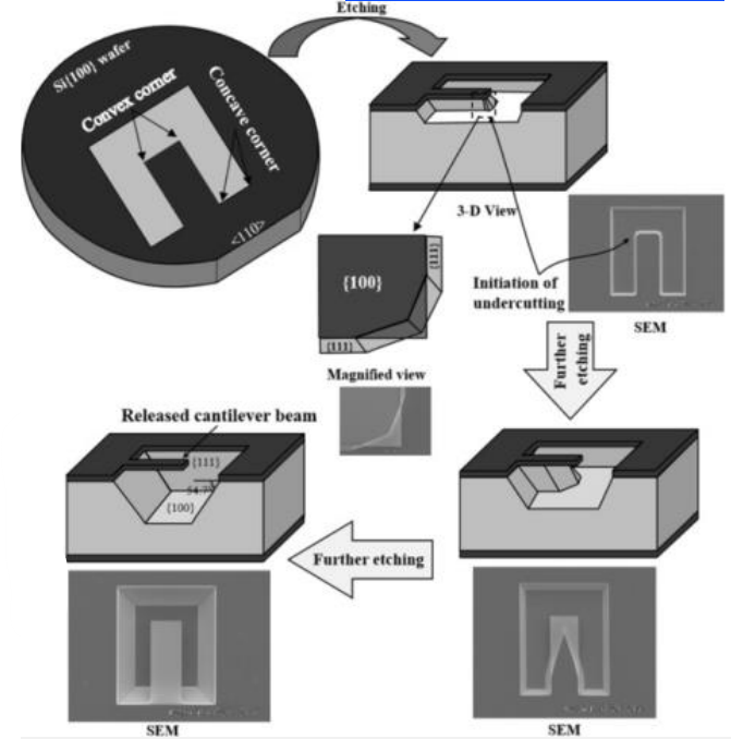
Bulk micromachining
Bulk micromachining is a process that consists in the selective removal of the bulk substrate to release suspended 3D structures. These structures are made of the same bulk material or of a thin film applied to it.
Bulk micromachining is less versatile than surface micromachining but allows for the removal of bigger regions.
Bulk micromachining uses the same techniques seen in wet and dry etching to release the desired structures.
P++ etch stop
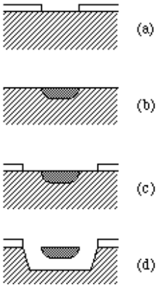
To stop the etching process, it is possible to create a heavily doped p region (darker in the image below), which etches really slowly compared to lightly doped or undoped silicon. The most selective etchant for this purpose is EDP.
Electrochemical etch stop
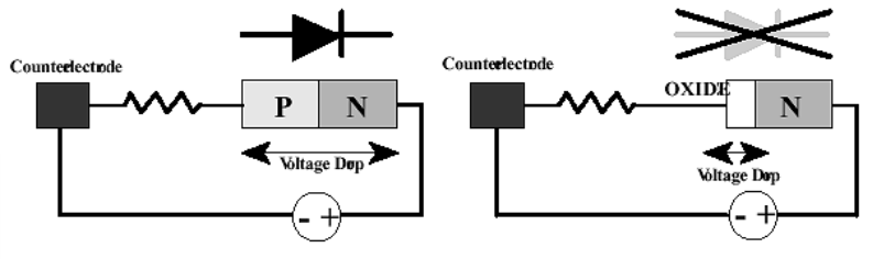
Electrochemical etch stop is another etch stop technique used in wet etching.
The process combines two effects: the first one is the fact that silicon oxidizes if a current flows through it, the second one is the fact that the etchant used has a high selectivity and doesn’t etch
The etch stop is provided by the use of a reverse biased p-n junction which stops the current flow as long as the p substrate isn’t completely etched. The result is that the position of the p-n junctions defines what is etched and what isn’t.
 The setup consists in an acid bath (
Surface micromachining
Surface micromachining is a technique that is used to form suspended microstructures out of thin layers of different materials. Compared to bulk micromachining this technique is more involved but also more versatile and it can provide better resolution.
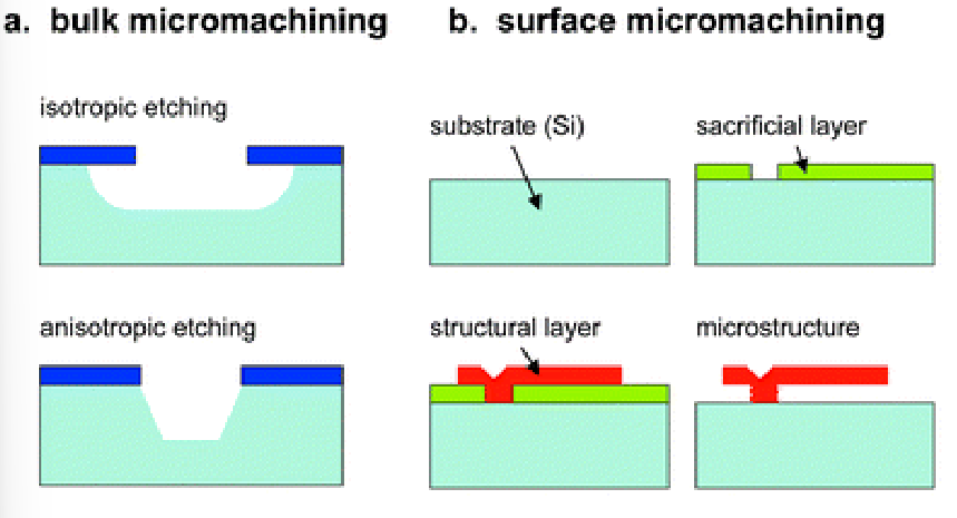
A key component that is required to perform surface micromachining are sacrificial layers, which are thin films required to support the structure to be formed during the process but that need to be finally removed. Opposed to sacrificial layers are structural layers which are the one that will remain after the end of the process.
Surface micromachining is often used to create MEMS.
Selection of materials and etchants
For what concerns the etchant it is obviously important to choose the one with the proper trade off between etch rate and selectivity. It is also important to select the right deposition temperature for the various layers that make up the structure. This consideration does not concern the sacrificial layer since it will be removed anyway. For optical applications it is also important to evaluate the surface smoothness left by the process.
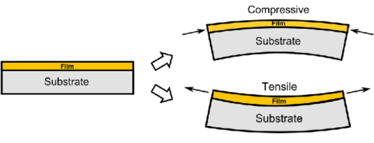
The last important thing to take into account is the intrinsic stress of the structural layer which could cause the rupture or the bending of the film once it is release from the rest of the material.
Evaporation drying
Release stiction
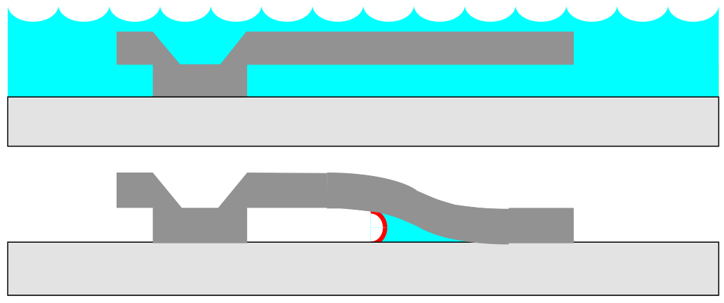
Another issue that can arise from the rinsing step is the fact that the microstructures can stick to the substrate due to Van der Waals forces and hydrogen bonding that cause the formation of a liquid meniscus. This is not an issue if the structures can be released after drying but this is not always the case.
To prevent stiction there are several possible solutions:
- Use low surface tension liquids such as methanol.
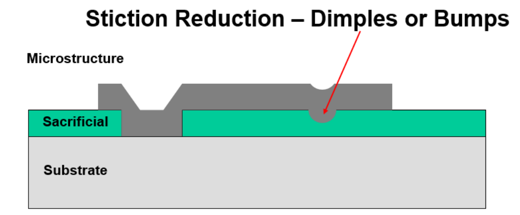
- Reduce the adhesion area by introducing dimples or bumps in the design.
- Integrate support microstructures that keep the features stable for the whole process and that can be removed in the end. An example of support structures are micro-fuses which can be electrically destroyed at the end of the process.
Another method could be evaporating the liquid to release the structures; the problem with this is that at microscopic levels crossing the liquid to gas boundary can cause too much stress. There are two possible ways to avoid this:
- Avoid passing from liquid to gas directly by exploiting sublimation drying. In this method the liquid is frozen and then the pressure is lower to sublimate the residue. This technique cannot be used with water since it expands as it freezes.
- Pass from liquid to gas by using
supercritical drying. This method passes through the supercritical region where there is no more distinction between liquid and gas. Since reaching the supercritical point requires high temperatures and pressures, which could damage the device, we usually use which has the supercritical point at ambient temperature.
The last solution is to avoid wet etching altogether and used vapor phase etching.

Wafer bonding
Wafer bonding is a technique used to stick two or more wafers one on top of the other to create complex mechanical systems that couldn’t be build in other ways. It is possible for example to create motors, sensors, pumps and so on but also for packaging.
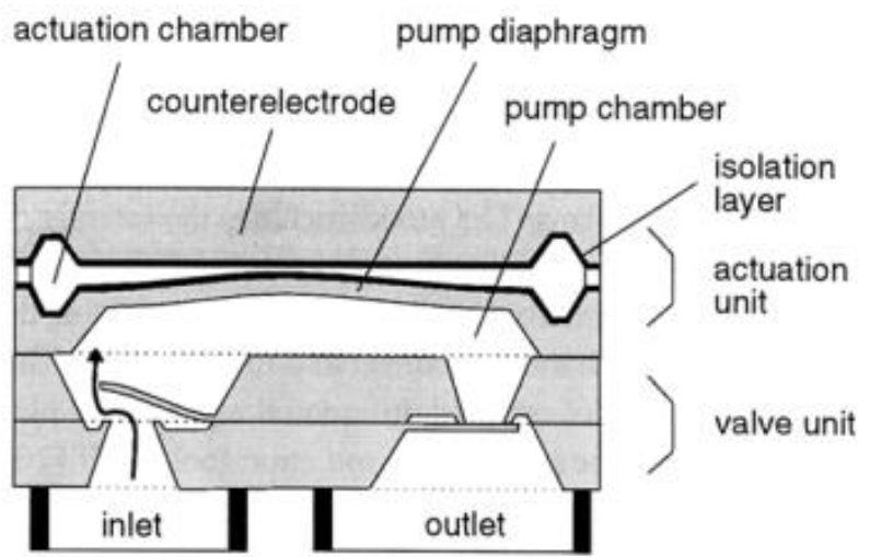
In the picture below we can see an example of micro-pump. The working principle is similar to the one of a normal pump but in this case the pressure difference is create by applying a voltage to a parallel plate capacitor with one flexible plate (dark horizontal lines). This causes the flow of liquid from the inlet to the pump chamber. When the pump diaphragm relaxes the inlet gets sealed by the pressure and the liquid can flow through the outlet.
There are three classes of wafer bonding:
- Heat assisted bonding
- Electrical field assisted bonding
- Chemistry assisted bonding
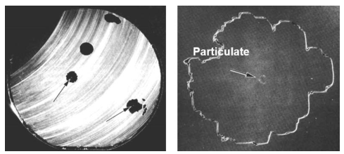
In all the cases it is fundamental to correctly prepare the surface before proceeding since even microscopic particles can create large defects in the final result. A 1
Fusion (or direct) bonding
Fusion bonding is used to bond together silicon based wafers (e.g.
The results are a nearly perfect high strength bond with only a nanometric
The process is simple and uses high temperatures and high pressures to bring the two polished surfaces in contact with each other.
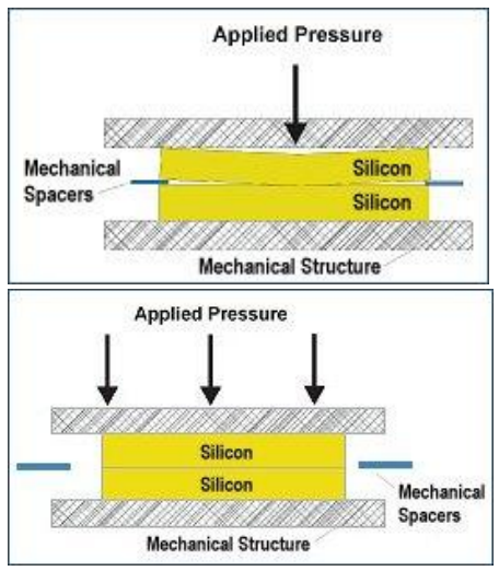
Since high temperature are involved, this method should not be used for wafers with temperature sensitive devices.
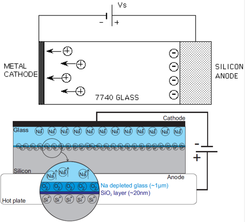
Anodic bonding
The field assisted glass-silicon sealing, also referred to as anodic bonding, is a process which permits the sealing of silicon to glass well below the softening point of the glass. For the method to work properly, the two surfaces must have a surface roughness of less than 0.1
The pieces to be bonded are assembled and heated on a hot plate at atmospheric pressure to a temperature between 400 and 500°C (a relatively low temperature if compared to fusion bonding). A DC power supply is connected to the assembly such that the silicon is positive with respect the glass. When a voltage on the order of some hundreds volts is applied across the assembly the glass seals to the silicon. No external force is necessary.
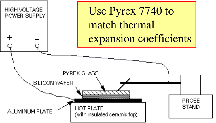
The main limitation of this method is that it requires the two material to have a very similar thermal expansion coefficient (for silicon we use Pyrex 7740). If this is not the case they would expand by different amounts during the heating phase and, when cooling down, they one of them would crack due to the stress caused by the other one.
Even though the temperature is lower compared to the previous case and there is no external load, the conditions are still very harsh and thus the process is not suitable for wafers with active components.
Working principle
The mechanism involved in the bonding process is attributed to mobile positive ions in the glass whose mobility is increased by the elevated temperature. The ions are attracted towards the cathode placed on the glass and this forms a negative charged region at the glass-silicon interface which pulls the two surfaces together, acting as the external load in the fusion bonding.
 It is important to constantly monitor the current to detect when the bond is complete and avoid breakdown.
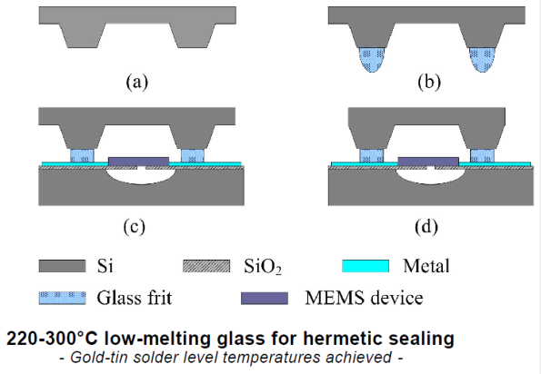
Glass frit bonding
This technique is different from the other two since it uses a sort of “glue” to bond the two surface together. This allows for lower temperature bonding (as low as 160
The fact that a external material is used to bind the two surfaces together has other advantages: we have a higher selections of materials to bind together, the glass frit can be patterned to achieve localized bonding, it can compensate for surface imperfections.
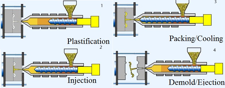
Micro injection molding
Micro injection moulding is a replication technique used to reproduce many pieces from a mould insert. The most used materials are thermoplastics such as PMMA, PVC and ABS but they can also be mixed with metals or ceramics to form sintered parts.
The process works similarly to classical injection molding: the thermoplastic is melted and injected into the molds by a reciprocating screw with a pressure ranging from 500 to 2000 bars. After the plastic has cured the mold opens and the parts can be ejected.
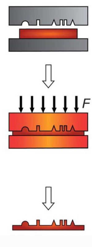
Hot embossing
Hot embossing is a technique similar to the previous one in the sense that it uses thermoplastic to form features according to a mold. In this case though the plastic is not injected but is heated just above its glass transition in place and pressed between the edged of the mold itself.
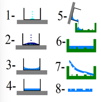
In situ casting
In situ casting is a method to form high resolution molds starting from a polymer such as Polydimethyl-siloxane (PDMS). PDMS is a flexible silicon which is cheap and easy to use.
The method to produce the cast consists in weighting the proper amounts of the curing agent and the base (PDMS is a bi-component). After mixing the two parts together they have to be degassed in a vacuum to remove air bubbles. After that the mixture can be poured in the cast where it self levels. Eventually, after waiting for the PDMS to cure, it can be demolded and the edges can be refined.
Global planarization
Global planarization is the technique that we saw in wafer production and it uses Chemical Mechanical Polishing (CMP).
CMP takes advantages of the synergic effect of both physical and chemical forces for polishing of wafers. This is done by applying a load force to the back of a wafer while it rests on a pad. Both the pad and wafer are then counter rotated while a slurry containing both abrasives and reactive chemicals is passed underneath.
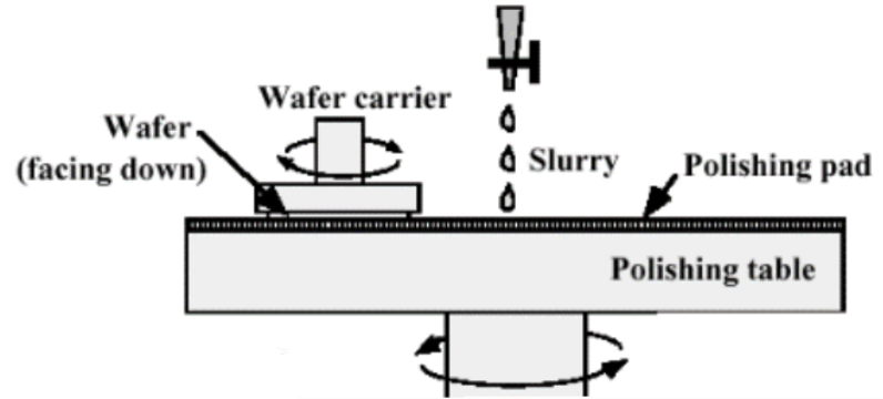
The important parameters of the process are:
- The pressure applied to the wafer
- The speed of rotation
- The etchant concentration
- The grain size of the slurry
Laser machining
Laser machining is a non contact technique that doesn’t produce internal stress in the processed material.
Lasers can be used for drilling, cutting, patterning and annealing of metals, plastics, ceramics, semiconductors and glass materials.
The smallest feature sizes can be smaller than a micron and surface roughness better than 100 nm. The radiation produced by the laser is absorbed by the substrate and generates locally very high temperature and pressure, which cause the material to be ejected.
The laser source must be properly chosen, so that the wavelength is absorbed by the material to be processed. The shape to be machined can be directly written by the laser beam, or defined on a mask and projected onto the workpiece.
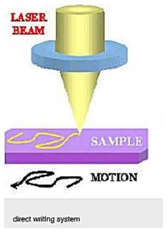
The main drawback of this technique is the fact that the process is slow and the machinery is expensive but this is compensated for by the fact that there is almost no limitation in materials, shapes and size of the features (compared to classical machining).
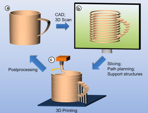
Additive manufacturing
Additive manufacturing is a process in which a digital 3D design is transformed into a physical object by building up multiple layers of some particular material. In order to do this, the design has to be virtually sliced so that a machine can lay the layers one on top of the other accordingly.
It is important to note that the final object will not be a perfect replica of the design but it will have some defects due to the loss of resolution of slicing.
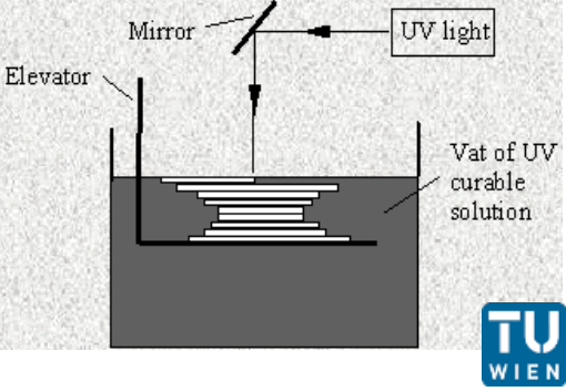
Micro stereolithography
In this process object are fabricated by building up hundreds of layers of hardened resin.
The process involves a light source (usually a UV laser) which scans the surface of a photosensitive resins that hardens if exposed to light. The first layer scanned is in contact with the bottom of a sliding table submerged in the resin. After the first layer is complete, the slider can move deeper in order to allow for another layer to be created.
Due to the sequential nature of the process, its applications are limited to prototyping since it would be too slow for manufacturing.
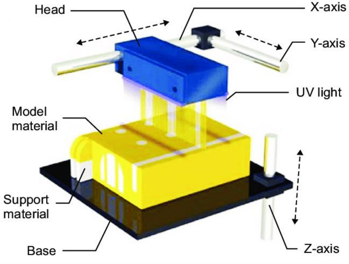
Inkjet printing
This technique is similar to the previous one (the object is built layer by layer), but in this case the layers are created by droplets of polymer dropped by the nozzles of a moving head. Similarly to the previous example, the resin has to be cured by a UV lamp after being deposited.
The advantage of this method is that the printer’s head can deposit two materials at the same time (from different nozzles): the building material and the support material. The support material is not part of the finished object but is required to support deposited build material in regions with voids or overhangs. The support material is usually soluble so that it can be fully removed when the process is complete.
In contrast to conventional stereolithography, where lightweight supports are only required in areas with severe overhangs, inkjet-based AM requires a completely dense support structure.
Two photon polymerization (2PP)
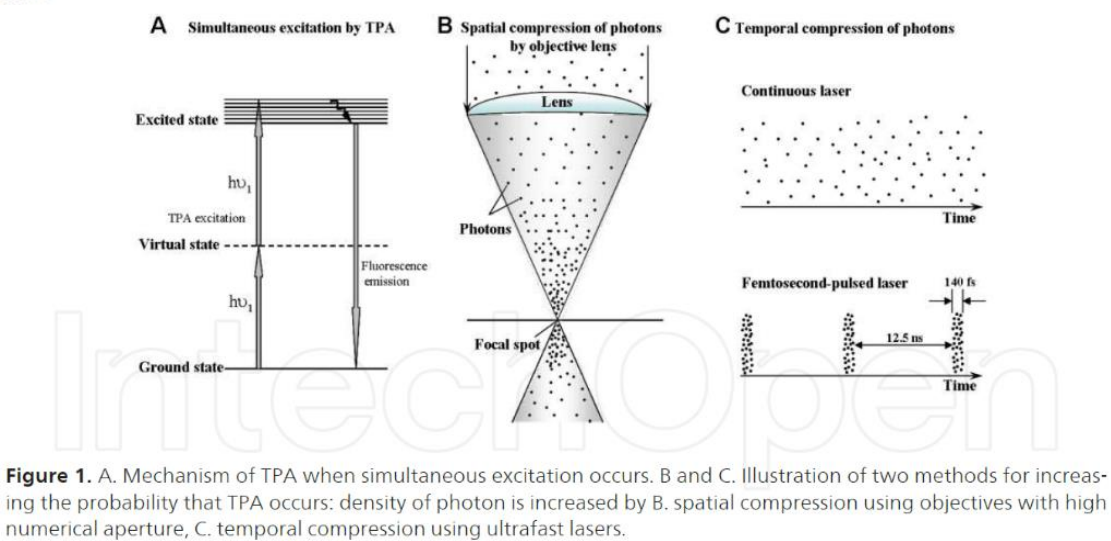
For two photons absorption to occur, photons must be present in sufficiently high concentration to drive a transition via a very short-lived (fs) intermediate virtual state to the excited state having energy roughly equal to twice that of the excitation wavelength (E = h
The idea is to shine a focus beam of light in a photo-resin which can be exposed only in the focal point (where two photon absorption occurs).
This technique allows to create build free-standing microscopic structures with feature sizes orders of magnitude beyond that of other lithographic techniques.
Differently from traditional stereolithography, 2PP is not a layer by layer technique since the focal point of the laser can be moved in any direction within the resin. For this reason it is considered a true 3D writing technique since it allows to create more complex structures than with layer by layer SLA