
CVD allows thin film formation from vapor phase reactants. The material that can be deposited range from metals to semiconductors to insulators.
All CVD techniques involve an energy source (usually temperature) that is used to break the precursors.
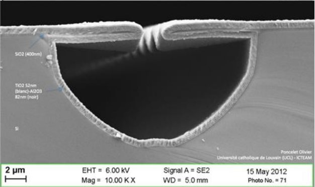
Acceptance angle and conformality
The number of molecules incident on the surface is a function of the acceptance angle. Since the number of molecules directly affects the growth rate, it is common to obtain uneven surfaces. The more even the thickness of the film, the more conformal the result is.
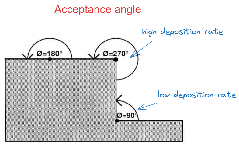
Even though a fully conformal deposition represents the ideal case, there are situations where conformality is not wanted.
High aspect ratio shapes (for example thin and deep holes) can generate voids during the CVD process if the conformality is not sufficient.

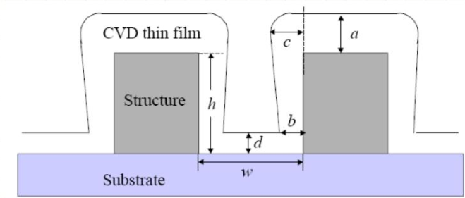
By referencing the image below we can define the following quantities:
- Aspect ratio =
- Conformity =
- Sidewall step coverage =
- Bottom step coverage =
- Overhang =
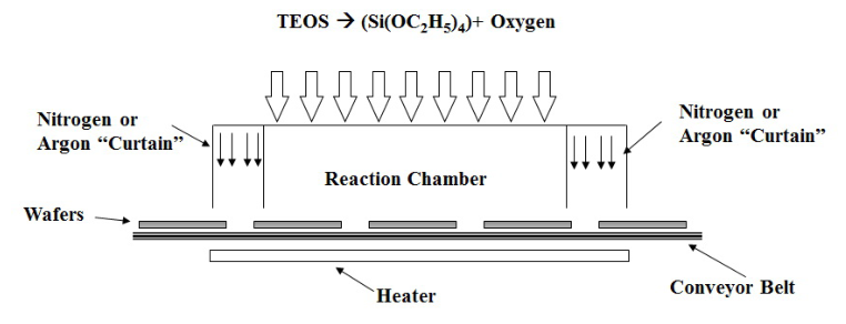
Atmospheric Pressure CVD (APCVD)
In APCVD wafers are placed on a conveyor belt that runs in an open chamber (there are no physical barriers, the separation with the outside is created by Nitrogen or Argon “curtains”). The atmosphere in the chamber is heated to favour the deposition of the materials in the gas.
Since the chamber is not enclosed, the process can go on continuously, increasing the throughput; the same fact, on the other hand, increases contamination.
Low Pressure CVD (LPCVD)
LPCVD is similar to APCVD but in this case the reaction happens in a sealed environment, increasing uniformity and purity. Because of the low pressure of the gas, the concentration of molecules to be deposited is lower and thus the deposition rate decreases compare to APCVD.
Plasma generation
DC voltage
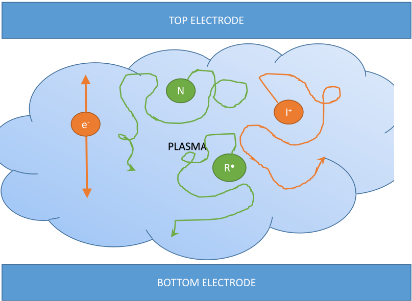
Plasma is generated by applying a voltage to cathode and anode and placing a gas of neutral particles between them. The voltage accelerates the free electrons which collide with the atoms of the gas.
Electrons have the following effects on the gas:
- They can ionize the atoms of the gas freeing an extra electron, generating a cascading reaction.
- They can also dissociate the molecules generating free radicals which are extremely reactive.
- They can excitate the atoms in the gas making their electrons jump to a higher energy level.
- When the excited electrons return to ground state (relaxation) they emit visible light (which is the main sign of the formation of plasma).
AC voltage
The steps are the same as in the previous case but this time the AC voltage causes the electrons to oscillate and does not affect the ions (which are too massive). It is also possible to introduce a bias voltage to accelerate the ions in one direction.
Plasma Enhanced CVD (PECVD)
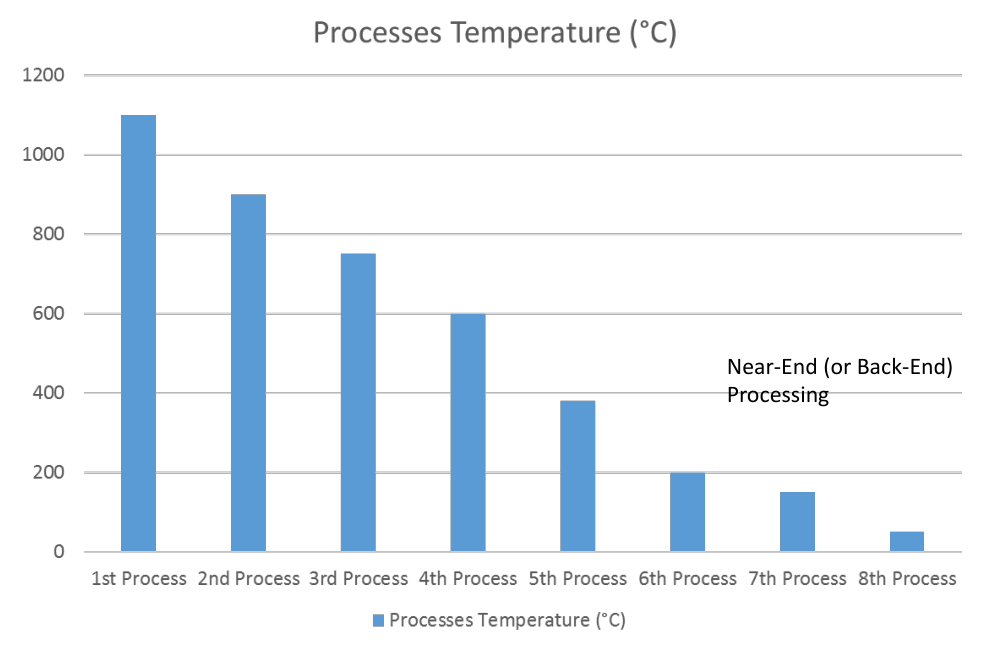
Plasma is used in CVD to force reaction that would not be possible at lower temperatures and deposit ions and free radicals without having to heat the substrate. This offers more degrees of freedom for near the end processing: using high temperature could in fact damage or destroy previous steps. The disadvantage is that plasma can contaminate or damage the substrate.
PECVD offers also the advantage of having a higher deposition rate compared to LPCVD but the plasma can damage or contaminate the wafer.
CVD techniques comparison
| Type | Advantage | Disadvantage | Temperature |
|---|---|---|---|
| APCVD | Simple, Fast | Contamination, Poor step coverage | 350-1200 C |
| LPCVD | Clean, Conform, Uniform | High temperature, Slow | 550-600 C |
| PECVD | Low temp, High deposition rate, Good step coverage | Contamination | 300-400 C |
Atomic Layer Deposition (ALD)
Atomic Layer Deposition (ALD) is a modified CVD process to create an additional single atom layer on top of a substrate. The process uses several gases that are introduced into the reaction chamber one after the other.
Each gas reacts in such a way that the current surface is saturated (self-limiting reaction at the surface with first gas), and therefore the reaction comes to a standstill. Between the reactions of these gases the chamber is purged with an inert gas, like nitrogen or argon.
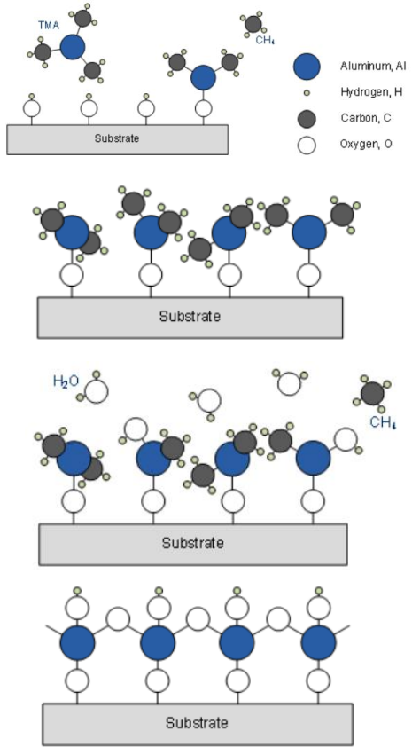
A specific example for an ALD process is the deposition of aluminum oxide, this can be realized with trimethylaluminum (TMA,
- First step is the elimination of hydrogen atoms which are bound to oxygen (simply because environment humidity) at the wafer surface. The methyl groups (
) of TMA can react with the hydrogen to form methane ( ). The remaining molecules bond with the unsaturated oxygen. If these atoms are saturated, no more TMA molecules can react at the surface. - The chamber is purged and subsequent water steam is led into the chamber. Every hydrogen atom of the
molecules now can react with the previously deposited surface atoms to form methane, while the hydroxyl anion is bond to the aluminium atoms. Hence, there are new hydrogen atoms at the surface which can react in a afterwards step with TMA like in the beginning.
ALD can achieve 100% conformality even in 3D structures and the thickness of the film can be precisely controlled by varying the number of cycles.
Silicon dioxide
Silicon dioxide can be deposited using CVD to obtain complementary results compared to thermal oxidation. Examples of these applications are the separation and insulation of different metallic layers, the creation of masking layers for implantation or to increase the thickness of a thermally grown oxide.
The reaction takes place in a chamber similar to the ones seen for epitaxy and the gases used are
Silicon dioxide methods comparison
This table is simplified compared to the one on the slides
| Property | PECVD | LPCVD | Thermal oxidation |
|---|---|---|---|
| Deposition Temperature | 200 | 450-900 | 1000 |
| Composition | |||
| Film density/quality | Low | Medium | Good |
| Step coverage | Non-conformal | Conformal/Non-conformal | Conformal |
Polycrystalline silicon (Poly)
Polycrystalline silicon can be obtained through LPCVD and is used as the gate electrode in MOS devices because it is more affordable than
The grain size depends on the deposition temperature: hotter deposition leads to larger grain structure (more similar to crystalline silicon), similarly to what happened in epitaxy.