Overview
High Electron Mobility Transistors (HEMTs), also known as Modulation-Doped Field Effect Transistors (MODFETs), are a type of Field-Effect Transistor (FET) that utilizes an heterostructure to achieve very high speeds in electronic devices. Their design and operation principles exploit the unique properties of semiconductor interfaces, especially the formation of a two-dimensional electron gas (2DEG) with exceptionally high electron mobility.
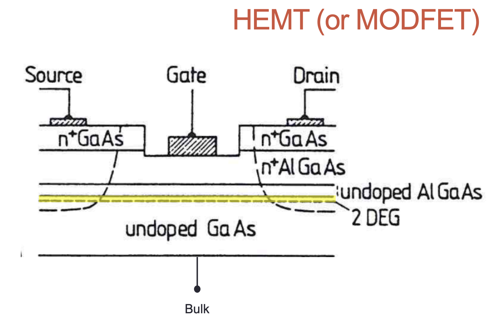
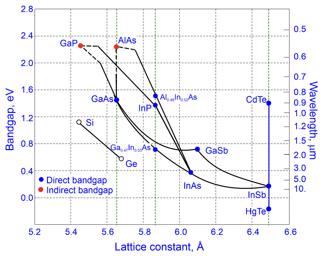
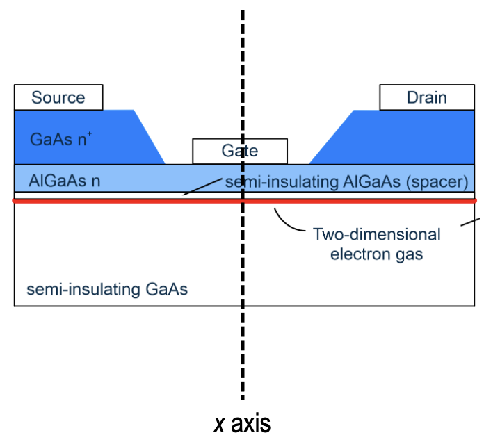
HEMTs are built using an heterostructure, typically made of materials like Gallium Arsenide (GaAs) and Aluminum Gallium Arsenide (AlGaAs). These materials are chosen for their different bandgap energies and their lattice compatibility, which allows for high-quality interfaces.
On a substate of semi-insulating GaAs , a weakly doped or undoped AlGaAs is grown epitaxially, then a wide bandgap n-doped material is deposit on top.
The key feature of HEMTs is the modulation doping technique. The wider bandgap material (AlGaAs) is doped with donor atoms (e.g., Silicon), which provide extra electrons. However, because of the band alignment at the AlGaAs/GaAs interface, these electrons transfer to the undoped, narrower bandgap material (GaAs), where they form a 2DEG. Typically, a thin layer of undoped AlGaAs (the spacer layer) is placed between the doped AlGaAs and the GaAs layer. This spacer helps in separating the free electrons (in GaAs) from their parent donor ions (in AlGaAs), reducing scattering and thus increasing electron mobility.
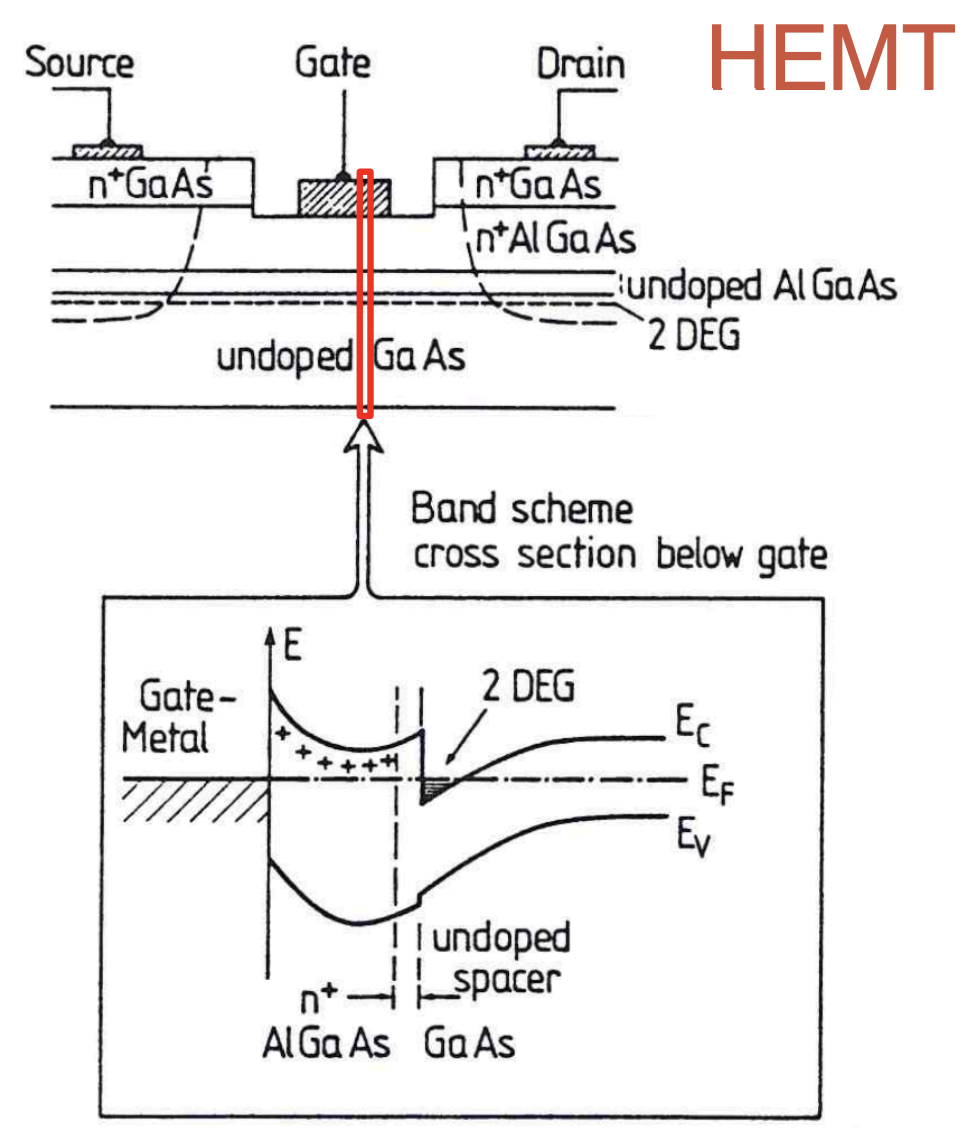
the space is wide more or less 20-100Å
Advantages of HEMTs
Note that in a N-type semiconductor the greatest source of scattering for electrons donated from donor impurities are the impurity sites themselves. In this case, the donated electrons are removed from the N-type SC and “exported” to an almost intrinsic SC. This arrangement is a clever way to drastically reduce donated electron scattering.
Electron mobility is very high for the 2DEG electron gas (up to
Due to their high electron mobility, HEMTs can operate at frequencies up to several hundred GHz. Furthermore HEMTs exhibit low noise characteristics at high frequencies, which is crucial for applications in receivers and other sensitive electronic equipment.
Contacts
Source and Drain contact must be prepared and create in such a way that there are deep and reach zone of highly n-type material, and the source and drain must form ohmic contacts with the semiconductor material where the 2DEG is located (at the interface). In contrast the gate electrode (diameter < 0.5
Note
Ohmic Contacts
Ohmic contacts are electrical connections that have a linear current-voltage (I-V) characteristic, meaning that the current through the contact is proportional to the applied voltage. Ohmic contacts are desirable for low-resistance and high-speed devices, as they do not introduce any voltage drop or power loss. To form an ohmic contact, the contact metal and the semiconductor must have similar work functions, or the difference must be compensated by doping or annealing.
Note
Schottky Contacts
Schottky contacts are electrical connections that have a nonlinear I-V characteristic, meaning that the current through the contact depends on the polarity and magnitude of the applied voltage. Schottky contacts are useful for rectifying and switching devices, as they have a low forward voltage and a high reverse breakdown voltage. To form a Schottky contact, the contact metal and the semiconductor must have a large work function difference, creating a potential barrier at the interface.
At thermal equilibrium the band diagram along the intersection normal to the layers below the gate electrode appears as below:
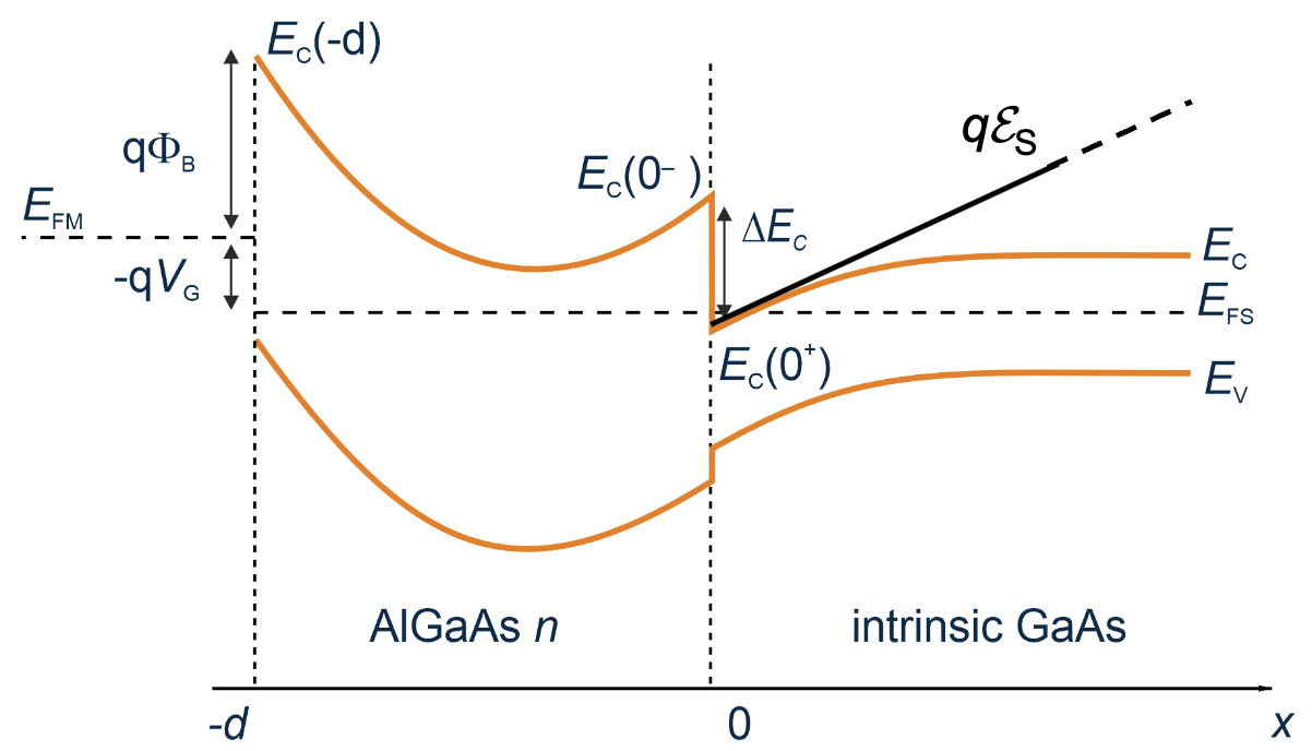
the gate electron witch is use to control the conductivity of the channel, is electrically isolated form the 2DEG by the depletion region formed by the Schottky junction.
when a positive voltage is apply between drain and source an electric field is created changing the band diagram at the interface and forcing the electron in the channel to move from the source towards the drain. Instead the gate voltage is utilised turn on or off the device.
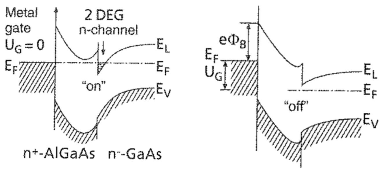
Due to the strong Schottky depletion layer, donors in the AlGaAs layer has been depleted and this leads to the fact that the most of the voltage drop occurs in this layer, creating a quasi-insulating layer barrier between gate and 2DEG. Depending on the gate voltage the triangular well is lowered (
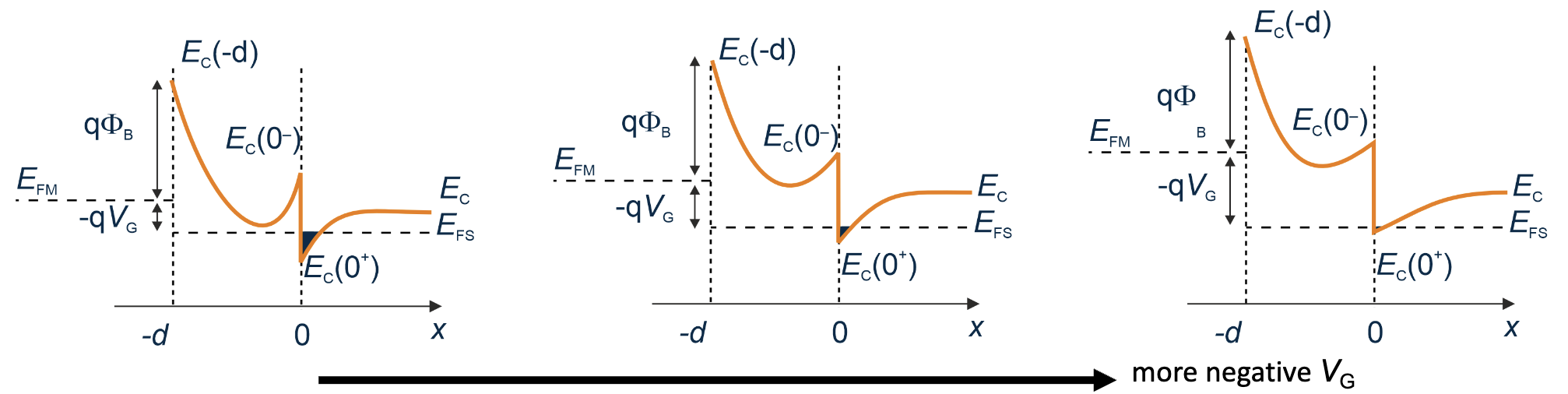
this changes the carrier density of the 2DEG switching the source-drain current.
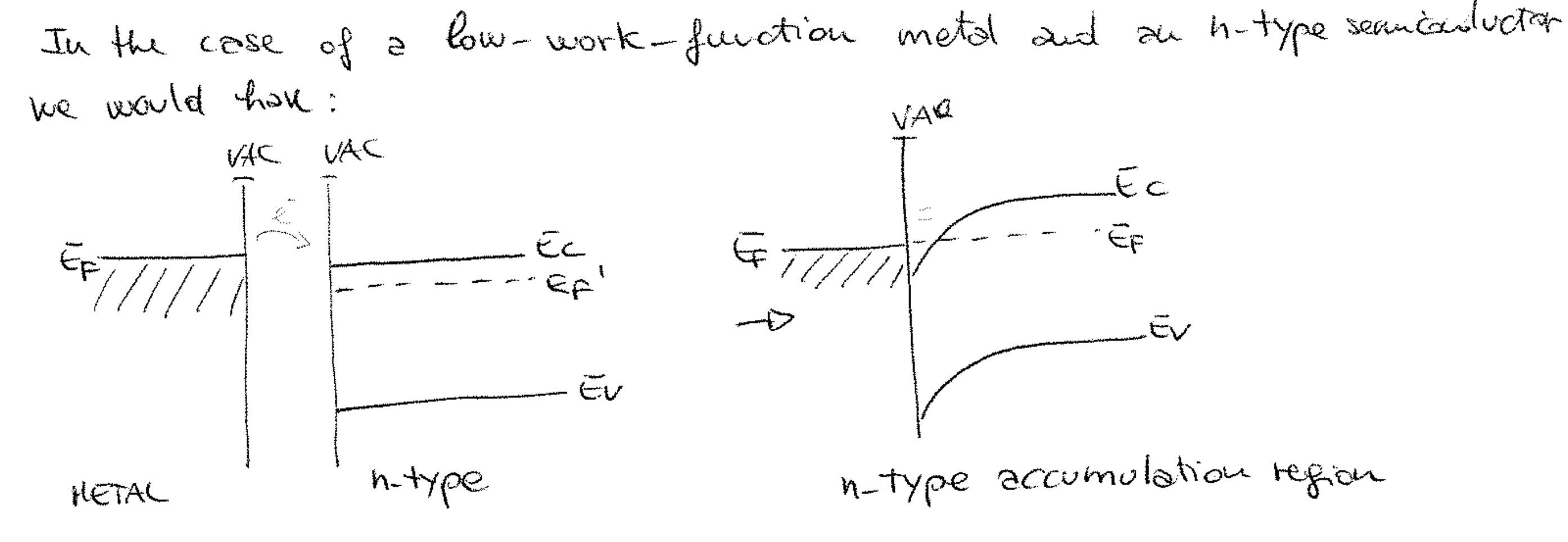
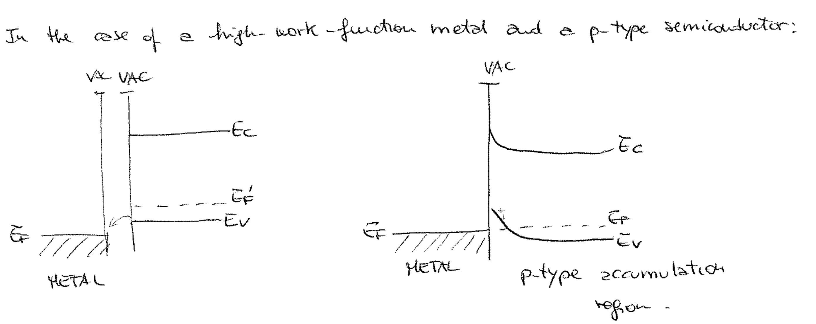
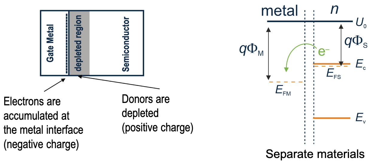
Metal-semiconductor junction
Depending on the work function of the metal
In the case in witch
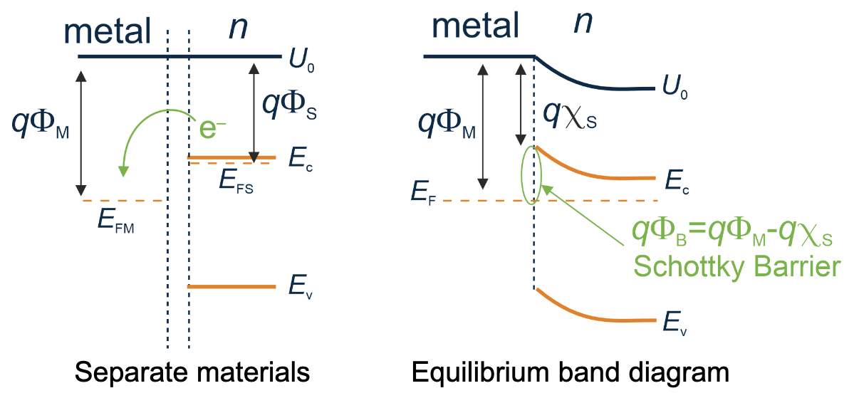
The metal introduces a charge distribution at the interface due to the transfer of electrons from the semiconductor to the metal to align the Fermi levels upon contact. This results in a depletion region within the semiconductor where free charge carriers are reduced and immobile donor or acceptor ions are left exposed. In a Schottky junction, the electric field is typically strongest within the depletion region. The strength and extent of this field, and hence the degree of band bending, are determined by the amount of charge and the permittivity of the semiconductor material, as described by the Poisson equation:
in this scenario the space of positive charged ions donors is balanced on the metal side by a corresponding excess of electron in extending over an atomic distance (at the interface). The maximum band banding at the interface is related to the Schottky barrier