What are heterostructures?
Heterostructures are semiconductors composed of more than one material. And a heterojunction is where the two materials meet.
Factors to consider when joining two semiconductors:
- BandGap
- Lattice mismatch
- Crystal structure
For good basic level heterostructure we usually need:
- Same crystal structure
- Similar lattice parameter
For this reason we usually use III-V group semiconductors, because they generally share the same crystal structure (diamond-like)
![[material_bandgap.png|]]
The prevalent use of heterostructures often involves combining gallium arsenide (
Purpose
The whole point of growing heterostructures is the opportunity that they offer to manipulate the behaviour of electrons and holes through band engineering creating for example wells to confine electrons.
How to build a band diagram of a heterojunction
Intrinsic semiconductors
Consider two materials A and B with

where
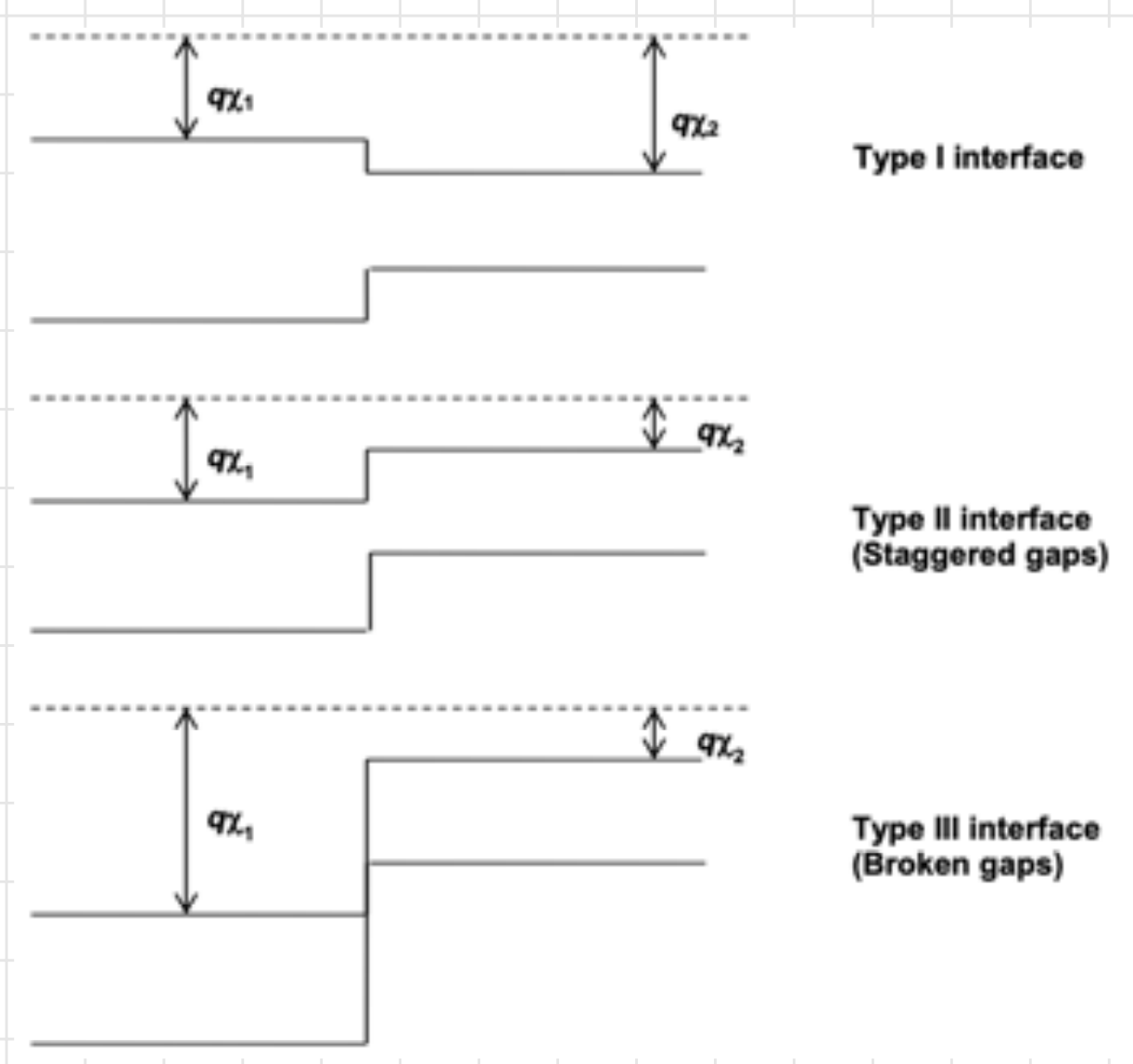
Further complication
The components of a heterostructure may have minima in the bands at different points in the Brillouin zone.
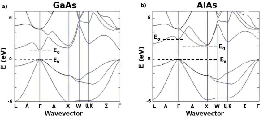
The effective mass and valley degeneracy vary abruptly at the crossover, and the change from a direct to an indirect energy gap gives a profound change in the optical properties.
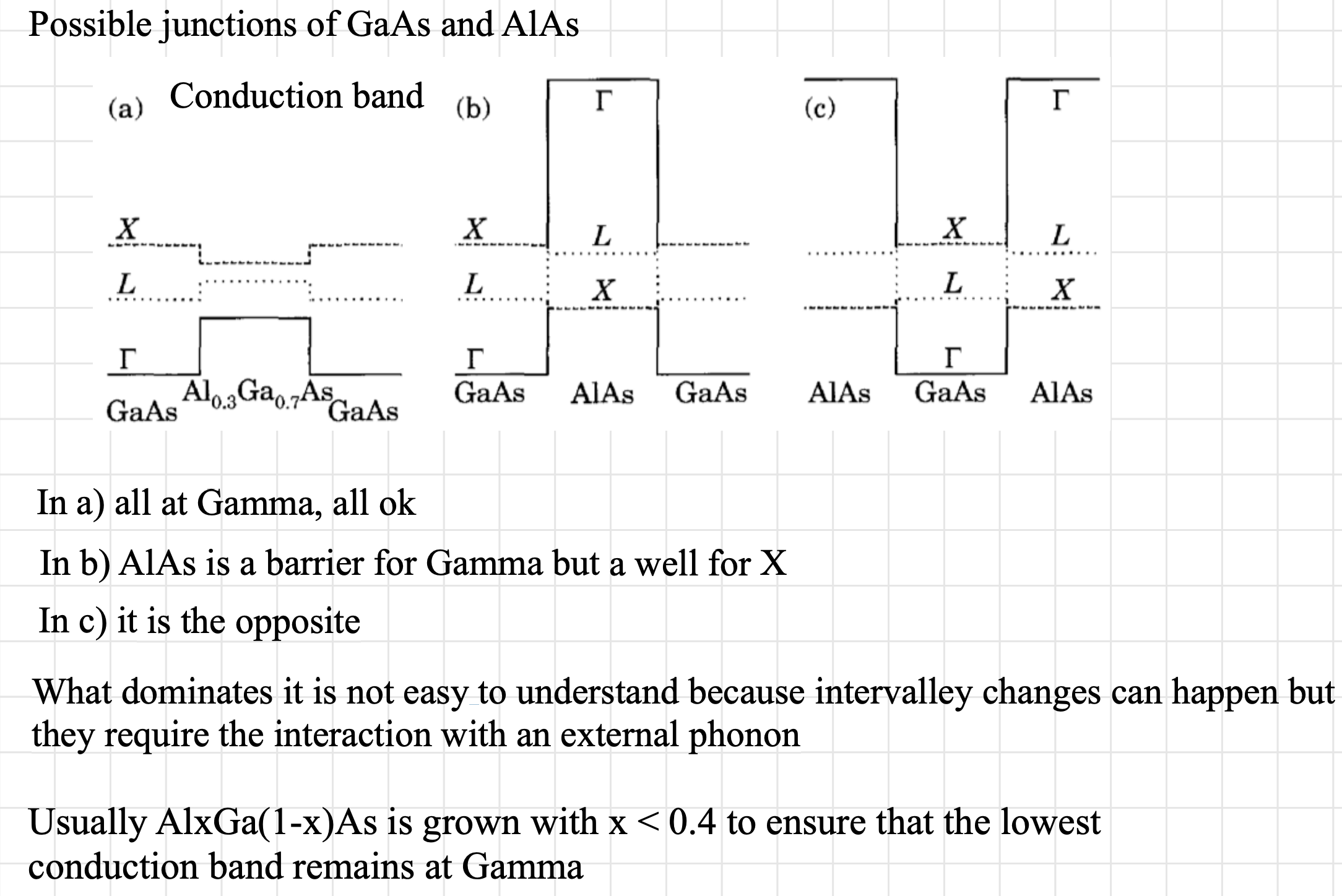
This configuration leads as we have seen to more unpredictable behaviour.
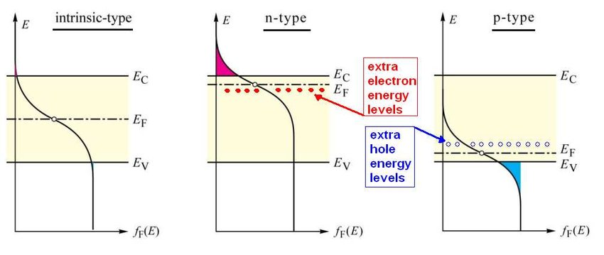
Doped semiconductors
Semiconductors can be doped. This changes the position of the Fermi level within the gap.
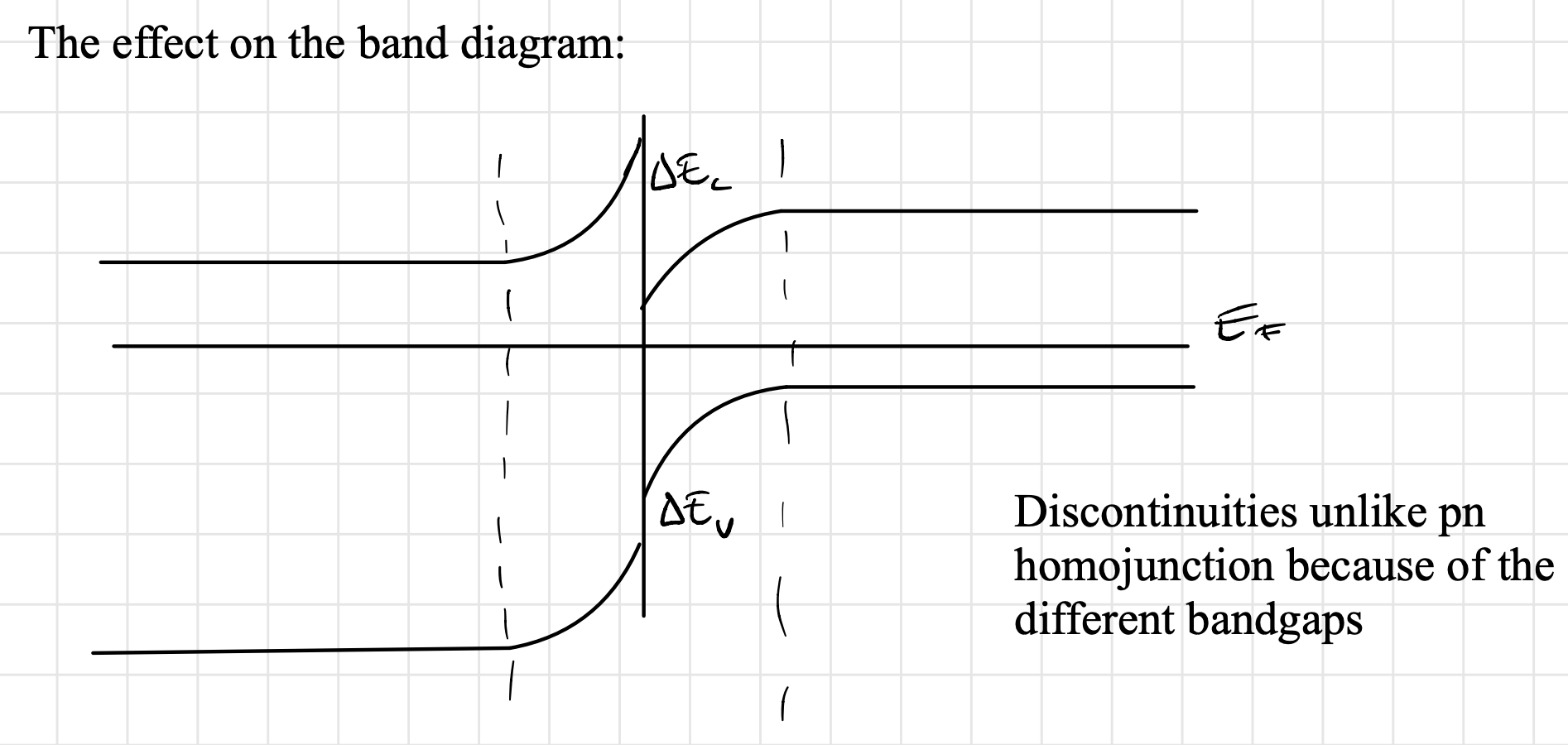
Depletion region
A depletion region is an insulating region within a conductive, doped semiconductor material where the mobile charge carriers have diffused away, or were forced away by an electric field. The only elements left in the depletion region are ionized donor or acceptor impurities. This region of uncovered positive and negative ions is called the depletion region due to the depletion of charges carriers, leaving none to carry the current. This region is formed at the interface of the heterojunction.
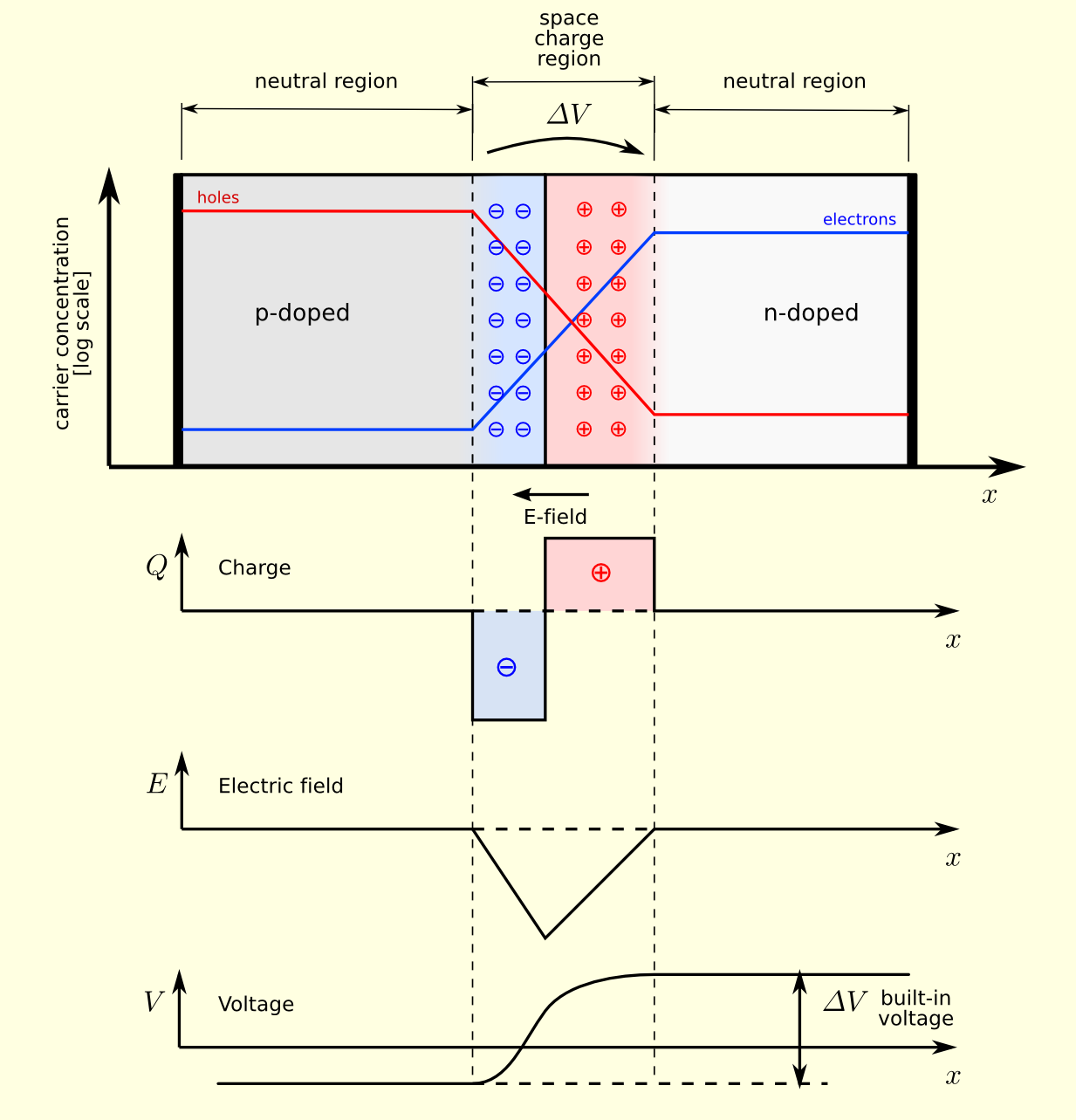
Out of equilibrium, the Fermi level exhibits two distinct values: one for the p-type material and another for the n-type. However, at the junction, electrons begin to diffuse from the n-type to the p-type, and vice versa for holes, resulting in the formation of a depletion region. This region induces band bending, explaining why the Fermi level remains constant at equilibrium.
If we examine an n-type material alongside a p-type material, with the n-type material possessing a bandgap greater than that of the p-type material

we obtain the following effect on the band diagram