
Goals
- We want to obtain an extremely pure piece of semiconductor (impurities
) to be able to control doping and consequentially the electrical properties. - The crystals need to have a regular structure.
- We want a monocristalline structure.

Production of silicon monocrystals
- We start the process with
or silica sand which contain a large number of impurities. - The sand is refined in a furnace @ 2000
C for ~ 8 days. This process produces 98% pure silicon which can be used in metallurgy (Metallurgic Grade Silicon MGS). - To improve the purity, MGS is crushed and reacted with
to obtain TCS (trichlorosilane) which is liquid at room temperature. This is done because it would be impossible to further purify solid MGS. - TCS is treated with a process similar to the one used to refine oil called fractional distillation which is the separation of a mixture into its component parts, or fractions. Through this process we obtain purified TCS.
- Silicon can be extracted from the TCS via the Siemens process that consists in creating a TCS and
vapor which is introduced in a chamber where the can deposit. After this steps we have reached the required purity level. 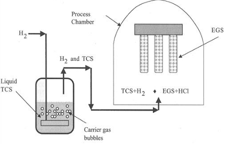
- Now that we have a hyper pure
we can transform it into a monoscrystal using the Czochralski process (CZ). The process consists in heating the slightly above its melting temperature (1415 C) inside a quartz crucible. Once the is molten, a small monocrystalline seed is put in contact with the melt, rotated and slowly pulled up. During this process part of the liquid solidifies and sticks to the seed, allowing it to grow with a diameter inversely proportional to the pulling speed. The rotation inhibits the natural tendency of the crystal to grow along certain orientations and to produce a faceted crystal. The orientation of the seed determines the orientation of the crystal to be produced. The process can take up to 3 days and in the end an ingot is produced. ^649cfb - The process can also be done with doped silicon. Adding a dopant introduces a new challenge because the concentration of dopant in crystal is not the same as that in the melt. We can define a segregation coefficient
where and are the concentrations. is generally , this means that the dopant tends to remain in the melt and thus its concentration increases during the process. Since this cannot be avoided the ingot produced will have different properties depending on where it is cut.
- The process can also be done with doped silicon. Adding a dopant introduces a new challenge because the concentration of dopant in crystal is not the same as that in the melt. We can define a segregation coefficient
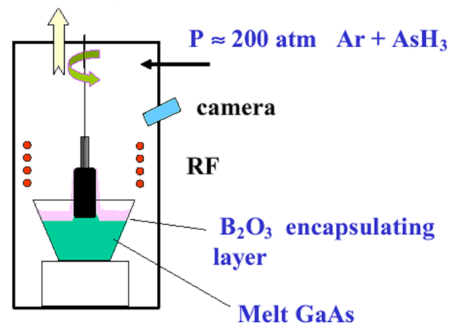
Production of III-V monocrystals
The Czochralski process has to be slightly modified (Liquid Encapsulated CZ) for growing
Wafer production
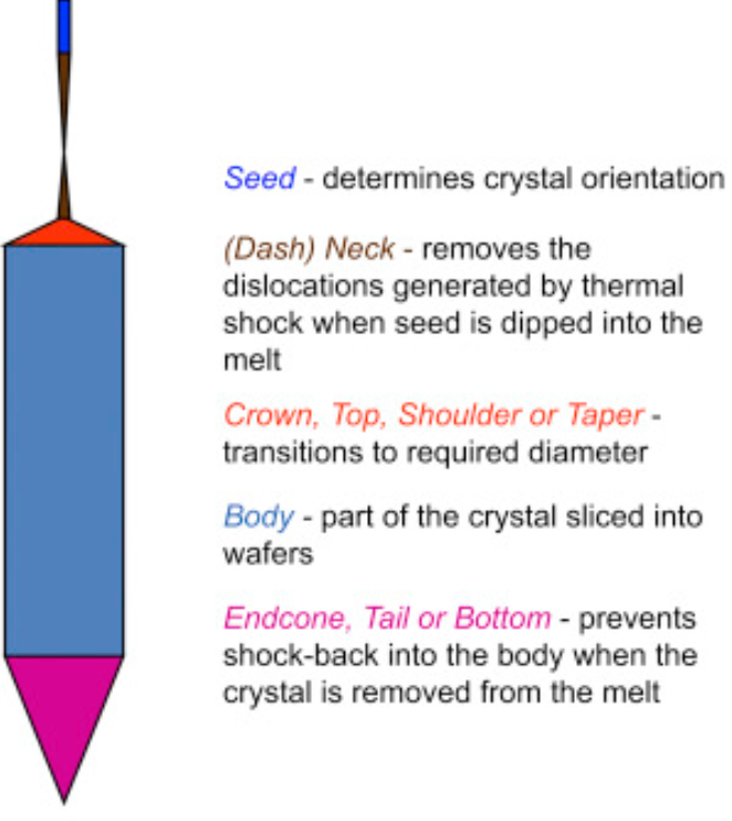
After the production of the ingot, a series of steps has to be followed to produce a usable wafer. The first thing to do is to crop the extremities of the ingot which contain defects and have a variable diameter.
Inspection
After that the ingot needs to be inspected to check that it is not undersized (an oversize ingot can be compensated for later), then the crystallographic orientation has to be checked through XRD (X-Ray Diffraction) and finally we have to measure the resistivities of the upper and lower faces to ensure that they are within spec (this step is necessary due to the variable concentration of dopant seen above). These three tests result in the rejection of ~50% of the ingots.
Shaping
If the ingot passed all the tests it can be shaped to refine the outer diameter and remove the waviness created during the pulling process.
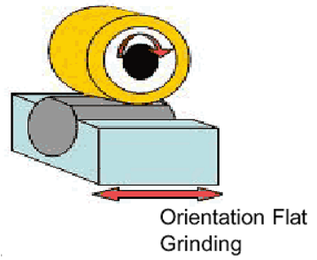
Flat(s) grinding
One or two flat zones on the edge of the ingot are ground to get a crystallographic orientation reference. This reference will be used to orient the wafer during the processing.
Ingot sawing
After all these steps the ingot is ready to be cut into wafers. The thickness of the slices can vary between 300
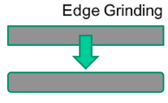
Edge grinding
After sawing the edges remain rough and have to be ground smooth to prevent crack and improve cleaning results.
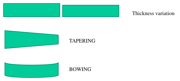
Lapping
The sawing process produced wafers that can have slight thickness and shape variation and this problem can be solved by grinding the wafers to make them flat.
Polishing
After lapping the wafers are mechanically flat but not optically flat (shiny). A mirror finish is required because it will allow to achieve better results in lithography and this can be obtained via a chemico-mechanical based polishing. Wafers can be Single Sided Polished (SSP) or Double Sided Polished (DSP).
Cleaning and marking
After the steps above the wafers can be cleaned with ultra pure deionized water to remove traces of the manufacturing process. In the end they are laser marked for identification purposes.