
Packaging is the process that transforms the finished wafer into a finished product by adding the necessary electrical connections and some enclosure that protects the delicate components.
Steps
First of all the an electronic map of all dies (chips) on the wafer is created (white marking) and the after a basic electric test the defective dies are marked so that they can be discarded later. After this step the wafer is sawn to separate the dies from each other.
After being separated from the wafer, the dies are bonded (attached) to the package and before fully enclosing it, it is fundamental to allow access to its electrical connections from the outside. This is done by bonding thin metal (
After that the package can be fully enclosed; the method depends on the material of the package: plastic packages are injection moulded around the die, while ceramic and metal packages use a lid and solder.
Finally a test is performed to make sure that they fully functional.
Functions of packaging
Packaging serves many purposes such as:
- Distributing power from the circuit board to the chip
- Distributing electrical or optical signals to and from the chip
- Dissipating heat
- Protecting the die from mechanical, chemical and electromagnetic concerns
Package types
There are multiple types of packaging types, classified depending on a number of parameters such as the connection density (the number of connections per unit area), the number of leads lines, etc.

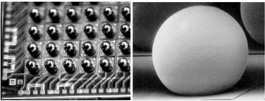
Flip chip bonding
One of the main issues with wire bonding is that wires are relatively long and thus can behave as parasitic components. For this reason there is a special types of packaging that uses flip chip bonding to minimize the distance between the die and the leads.
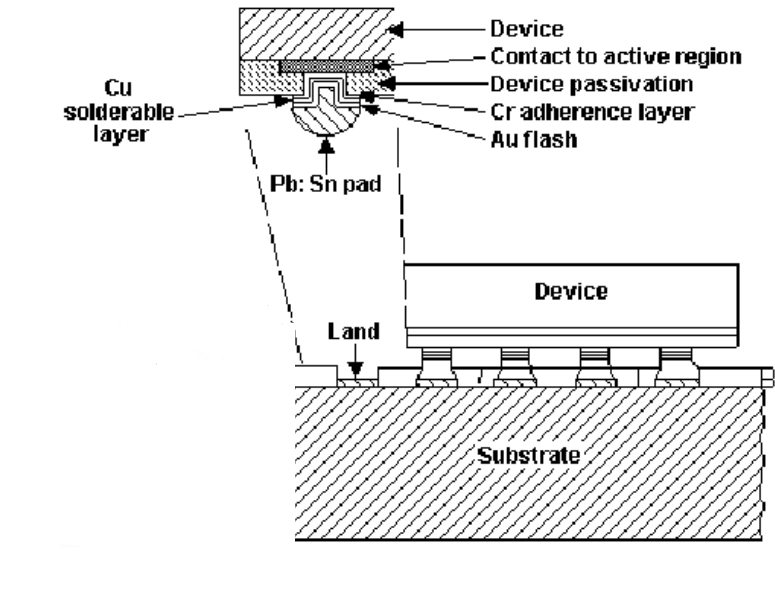
In flip chip bonding the die is placed upside down on the package substrate and it’s electrically connected to it by micrometric solder spheres.
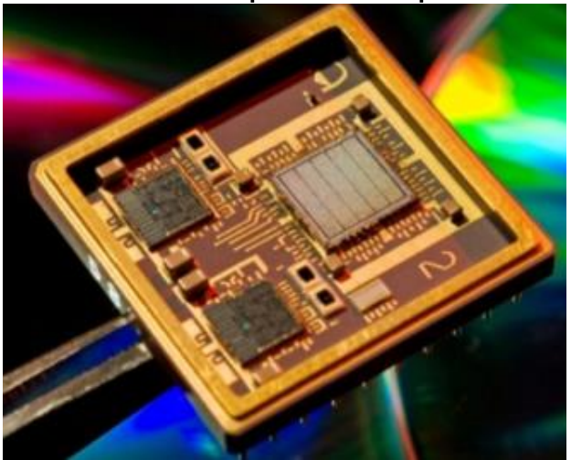
Multi chip modules
Multi chip modules, also called SoC (System on Chip) is a solution that solves the need for high connection density, high performance devices. This is possible thanks to the fact that multiple dies are bonded to a single substrate, minimizing the need for individual packages that would need to be connected by large PCBs.
There are two main definitions of multichip module:
- Some define it as a structure consisting of two or more integrated circuits electrically connected to a common circuit base and interconnected by conductors in that base
- A second approach to defining MCMs is based on the silicon efficiency achieved by the technology. Using this approach, an MCM is defined as a structure in which a packaging efficiency of greater than 30% is achieved. This definition implies a particular technology that allows chips to be packed closely together.
By efficiency we mean the density of chip packaging is determined by the ratio of silicon die area to printed circuit board area.
The main drawback of MCMs is the fact that the device becomes less and less reparable since it’s components are no longer independent. The advantages, on the other hand, are multiple: the space efficiency is increased, the parasitic components are reduced and thus performances are increased.
3D packaging
3D packaging is a further improvement of MCMs that tries to satisfy the requirements for high performance systems.
In this case multiple dies are stacked one on top of the other to minimize the footprint of the device.
To further reduce the size and improve the performance, it is possible to use a different kind of interconnections compared to the ones seen previously.
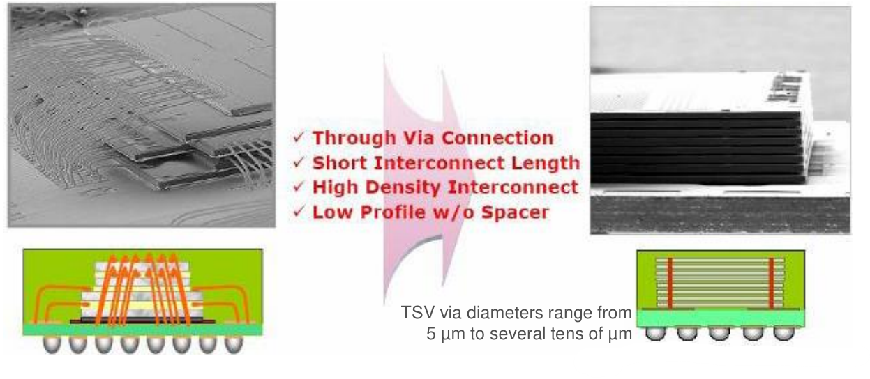
Instead of using wires to connect different dies, the connection are made through vias built directly in the silicon. This obviously requires a much higher degree of integration between the different components.