
Etching is the process in which unwanted areas of films or bulk material are removed selectively.
We can distinguish between wet etching, where the materials to be removed are dissolved in a chemical solution, and dry etching where they react with gases (thermal or plasma). In both cases the photoresist protects the areas which have to remain.
In some special cases, in place of a photoresist, there is the need to use a hard mask (usually made out of
Etchant properties
Different etchants can have a very different behaviour and etch the same material in various ways. The most relevant properties are:
Etch rate
The etch rate is the rate of material removal (usually in

Selectivity
Selectivity is the relative ratio of etch rate between what we want to etch (the film) and what we do not want to etch (mask, substrate, etc.).
It is important to notice that we usually have to consider two different selectivities: film/mask and film/underlying film.
We would like to have both values high to limit the resolution loss in the first case and the over-etch of the material in the second.
Unfortunately there is a trade-off between etch rate and selectivity: the higher the etch rate, the lower the selectivity (a very aggressive etchant will etch fast but it will also be less selective).
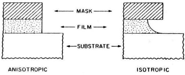
Isotropy
Isotropic etching means that the the etch rate is the same in all directions, while anisotropic means that there is some “preferred” direction where the etching will happen faster and others where it will be slower. The rate depends on the crystallographic plane of the material:
We have to keep in mind that isotropy is not only a property of the material, but also of the process: the same material can be etched both isotropically and anysotropically by selecting different etchants and different processes.
Less important parameters are:
- Surface roughness: different etchants can leave different surface finishes and this could be an important factor (for example) for optical properties.
- Control of etch parameters: the more control we can have on the end result the better.
- Safety: both reactants and by-products can be dangerous and need to be handled properly.
- Cost.
- Etch-stops effectiveness: it is important to have a way of knowing when to stop the etching process and often a time based approach is not enough. As we will see later, there are methods to precisely stop the process which allow to minimize the chance of over etching.
Wet etching
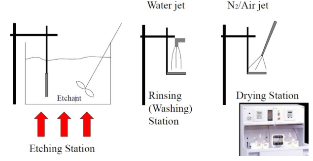
The wet etching process is mostly straightforward: the wafer is placed in an acid bath so that the etchant can come into contact with the surfaces that need to be etched. The etchant is stirred constantly to allow the removal of by-products from the etched regions. After the etching is completed, the wafer is rinsed (washed) in a deionized water jet and finally dried with a hyper pure
Wet etching silicon
Since silicon is a crystal, it naturally tends to etch anysotropically (some directions etch faster than others) but it is also possible to etch it isotropically using a multiple steps technique described below.
Isotropic silicon etching
One way to etch silicon isotropically is use to exploit the fact that
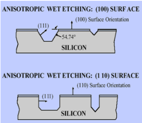
Anisotropic silicon etching
On the other hand, anisotropic etching of
Because of the presence of potassium, this technique cannot be used in microelectronics (in particular CMOS) because potassium can diffuse in the material and alter its electrical properties.
 Since
Since
The setup for the process is very simple since it only requires a hot plate, a Pyrex becker and a stirrer (a small magnetic bar covered in Teflon which is spun by and electromagnet) to improve by-product removal.
A poor by-product removal can increase the surface roughness due to a phenomenon called hillocking which consists in the formation of small unetched “pyramids” on the surface. These pyramids are caused by micrometric
Etching
We have seen before that for monocrystalline silicon we use two reactants for the etching process, in this paragraph we will talk about the hydrofluoric acid (
For what concerns the etch rate, this is strongly dependent on the concentration on the employed solution, the maximum available concentration is 49%, whose etch rate is on the order of
The main disadvantages of using this etchant is that its etch rate is not linear with high concentration and that it is very dangerous a dangerous acid: since it isn’t a strong acid and it looks like water, it doesn’t hurt if touched but will penetrate the skin and it will attack the bones.
Dependence on crystallographic plane
Dependence on temperature
Dependence on temperature
Dry etching
In dry etching the etchant comes from a gas or vapor phase source and its atoms are typically ionized in order to react better with the material to be etched.
There are two types of dry etching: plasma based and non plasma based:
Vapour etching
An example of isotropic dry etching process for silicon is Xenon difluoride (
The
The main disadvantages are that the etch rate is very fast the etching reaction is exothermic: this could be an issue to take into account since the heat could damage other features of the substrate.
Another method that can be used for vapor phase etching uses
Plasma based dry etching
Plasma etching has the advantage of being performed at lower temperatures compared to thermally driven reactions, it can provide directionality and introduces many degrees of freedom to the process.
The plasma is created similarly to what happened in PECVD with an RF voltage. In this case though the chamber is partially filled with the etchant in gaseous form.
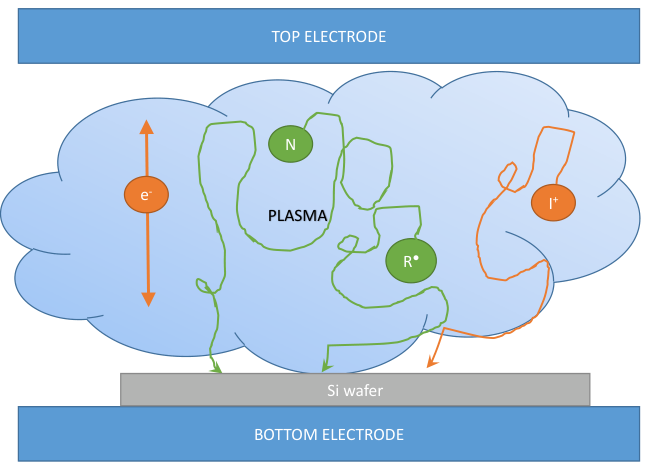
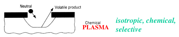
Since the chemical species will arrive at the substrate with random directions, the resulting etched profile will be fully isotropic, with significant undercut. In addition, the etch is purely chemical and, for this reason, it will also be selective: if some material (like the mask) is not etched by the specific free radicals, there will be no etch at all.
Reactive ion etching (RIE)
Reactive ion etching is a technique similar sputtering, but the noble gas is replaced with reactive gases which are able to selectively etch the target material. In both plasma etching and RIE, gas composition produces the reactive species necessary for etching.
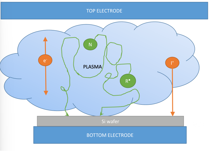
As we can see in the figure below in the right, the layout of the equipment is the same as in sputtering , but with the role of the two electrodes that it is inverted: the wafer is placed on the smaller power electrode on the bottom; on the top we have the bigger electrode connected to ground.
Comparing the picture above with the one for normal plasma based dry etching, we can see that ions (
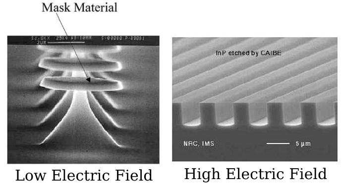
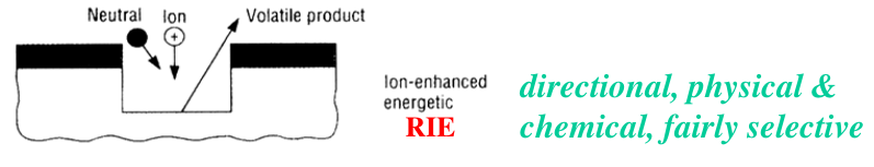 As we can see in the left, if we apply a low negative voltage (low bias voltage) we obtain something similar of an isotropic etching process, as we have seen in the previous classical plasma dry etching. On the other side, if we apply a high negative voltage (high electric field) we obtain a stronger acceleration of the ions, and, as a consequence, a more vertical bombardment of the substrate. The result is something which is impossible to obtain with other etching approach because it allows the tuning of the isotropy: increasing the bias voltage moves the process from a purely chemical, isotropic process, towards a purely physical, anisotropic process (we can imagine going from a classical plasma based etching to sputtering).
Inductively Coupled Plasma (ICP-RIE) Reactor
An upgrade of the RIE configuration is the one which is reported below:
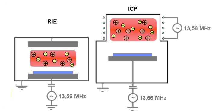
In Reactive Ion Etching we have a parallel plate configuration so as to generate plasma condition between the electrodes, and one single RF generator that is responsible for both the plasma generation and for the ion bombardment.
On the other hand, in Inductively Coupled Plasma, we have two RF generators that can be optimized independently in terms of electrical parameters: the top RF generator it is inductively coupled (13.56 MHz) with the reactor so as to generate the charge which creates the plasma. The bottom RF generator is coupled (13.56 MHz) with the bottom electrode, and it is purely responsible for the ion bombardment. This is a more complex system used for polysilicon etching and aluminium etching.
Selectivity
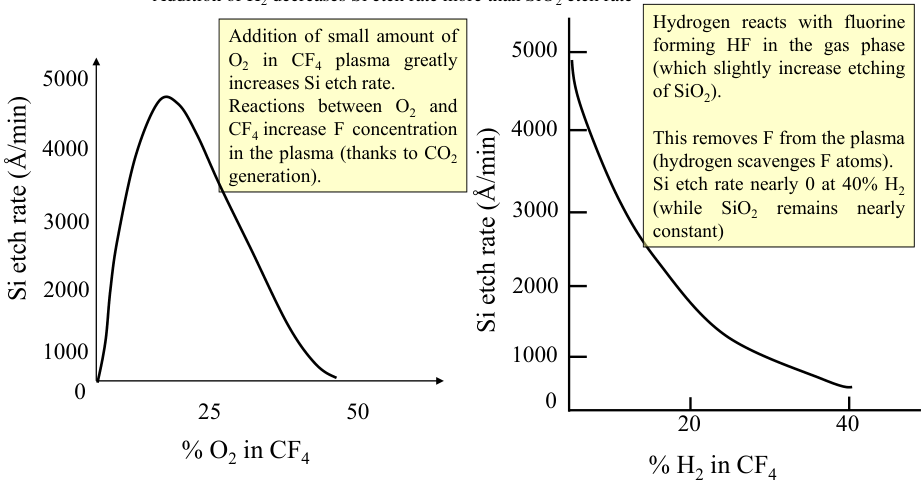
From the plot below we can see that starting with a pure 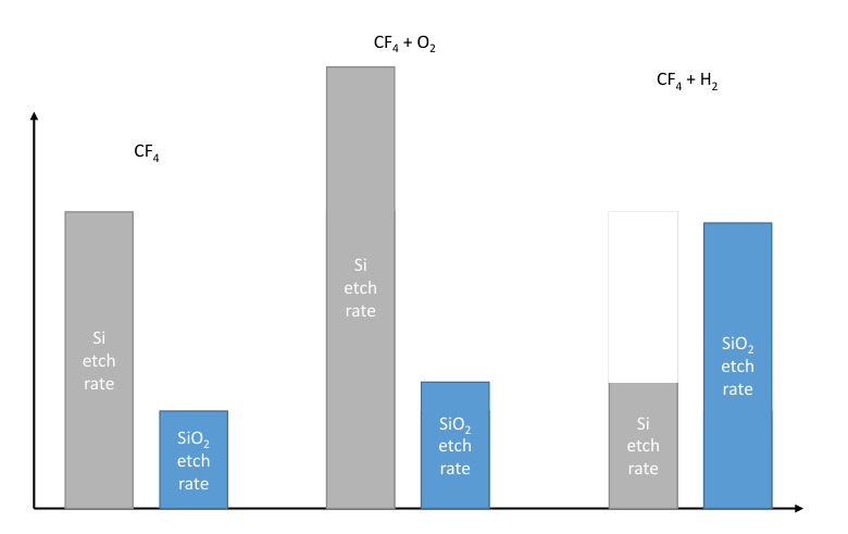
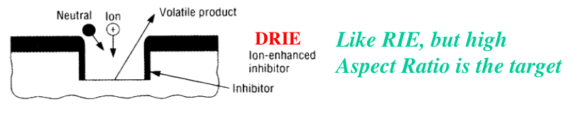
Deep Reactive Ion Etching (DRIE)
todo review
The standard processes uses a combination of fluorine (
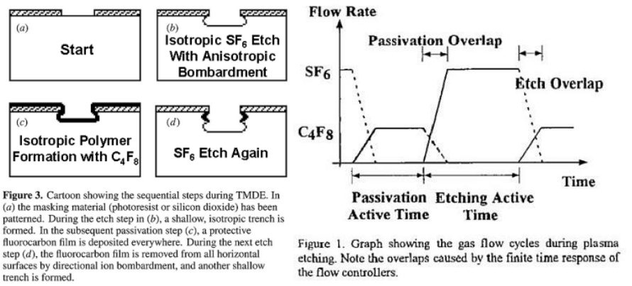
The etching step uses
A mixture of
Over-etch estimation
When planning an etching process, it is important to take into account the fact that the film thickness and the etch rate may not be uniform. This means that we need to over-etch to be sure to remove any leftover film. Obviously the higher the selectivity, the better the results since the substrate would be less affected.