Before analysing in more detail the crystals it is useful to have a general overview of the 3 different types of solids we can have.
Types of solids
| Monocrystal | Polycristal | Amorphous |
|---|---|---|
 |  |  |
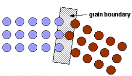
In a monocrystal all the atoms are arranged on a common lattice structure, in a polycrystal there are multiple lattices of the same type oriented differently to one another (each lattice is called grain), the interface between two grain is called Grain boundary. In amorphous material, on the other hand, the atoms are placed randomly in space.
While we will analyse mostly monocrystals, it is important to note that all three types are useful in practical applications, such as the creation of integrated devices.
Crystal structure
Bravais lattice
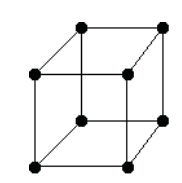
There are only 14 unique lattices possible in 3 dimensions called Bravais lattice. We are mostly interested in studying the cubic lattice which comes in three forms:
| Simple Cubic | Body Centered Cubic (BCC) | Face Centered Cubic (FCC) |
|---|---|---|
 | 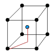 | 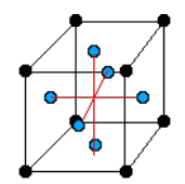 |
| the blue atom is in the center of the cube | the blue atoms are on the faces of the main cube |
Each lattice has a specific lattice parameter
Silicon lattice
Crystalline structure of
Miller indices
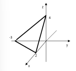
From what we will see later, the same material, with the same lattice structure can behave very differently depending on how it is cut (for thin films we are interested in the surface properties). To be able to describe different surfaces we can use Miller indices to identify the cut plane. The method to find those indices is as follows:
- Find the points where the cutting plane intercepts the
axes, in this case - Write the reciprocal of the numbers
- Reduce the list to the smallest integer
- Usually negative numbers are represented with a bar, the Miller index of this plane is
.
Surface behavior
The way the the crystal is cut influences in a very significant way the properties of the material. The cut can in fact change the number of dangling bonds on the surface, thus changing how reactive the surface can be (more dangling bonds speed up the oxidation for example). In the following table it is possible to see how different cuts change the surface properties of the same material.
| 111 | 110 | 100 |
|---|---|---|
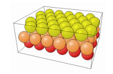 | 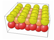 | 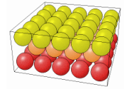 |
Crystalline defects
Point defects
| Type | Explanation | Image |
|---|---|---|
| Self interstitial | There is an extra atom of the right element |  |
| Interstitial | There is an extra atom of the wrong element | 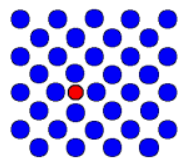 |
| Vacancy | An atom is missing | 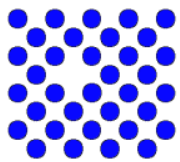 |
| Substitutional impurity | There is a wrong atom in the right place of the lattice | 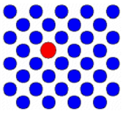 |
Line defects
The main line defect we will consider is edge dislocation which consists in the insertion of an extra half plane of atoms in the lattice. This half plane generates compression and tension stresses.
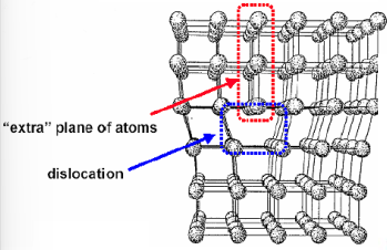
It is important to notice that dislocations can move across the material due to thermal or mechanical stresses.
Surface defects
The main surface defect we will consider are grain boundaries which are the interfaces between crystals with different orientations. The atoms on these boundaries tend to be loosely bound and thus more reactive. Lower temperature during the deposition process tend to create smaller grains and thus many boundaries, higher temperatures instead produce larger grains and less boundaries.
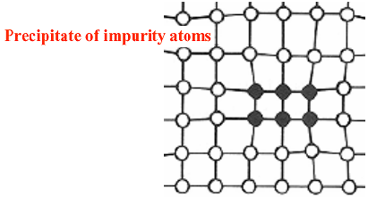
Volume defects
Impurities have an intrinsic solid solubility in the host crystal which varies with temperature; usually solid solubility decreases with decreasing temperature, so if impurities are introduced at maximum concentration for a certain T, when T is lowered some impurities (the excess respect to the solid solubility at that temperature) can precipitate and form local conglomerates. The volume of the crystal in that region can drastically change and this causes volume dislocations.