Lithography is a process used to select parts of the surface of a material that will need to be processed later with different technologies. One of the advantages is that it allows batch processing, i.e. the creation multiple similar features in parallel; this can drastically decrease processing times and thus decrease costs.
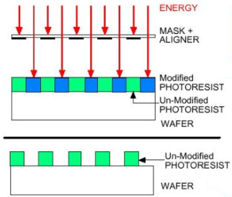
The process consists in covering the substrate with a photosensitive resists and partially covering it with a mask. After that the areas of the resists which are exposed to light will be modified and portions of the substrate will be exposed, allowing further processes to affect only specific parts of the substrate.
Resists
Composition
Photoresists are photosensitive organic mixtures which contain three main components:
- Inactive polymer resins (a binder that provides mechanical/chemical properties adhesion, chemical resistance, rigidity, thermal stability, etc).
- PhotoActive Compounds (PAC) which is what reacts to the energy source.
- A solvent which controls the viscosity of the base, keeping it in liquid state for spinning and thus affects thickness.
Resists also contain other elements that can be needed to improve specific properties, such as surfactants to allow them to stick to the wafer, dyes to absorb specific wavelengths, etc.
Properties
Polarity
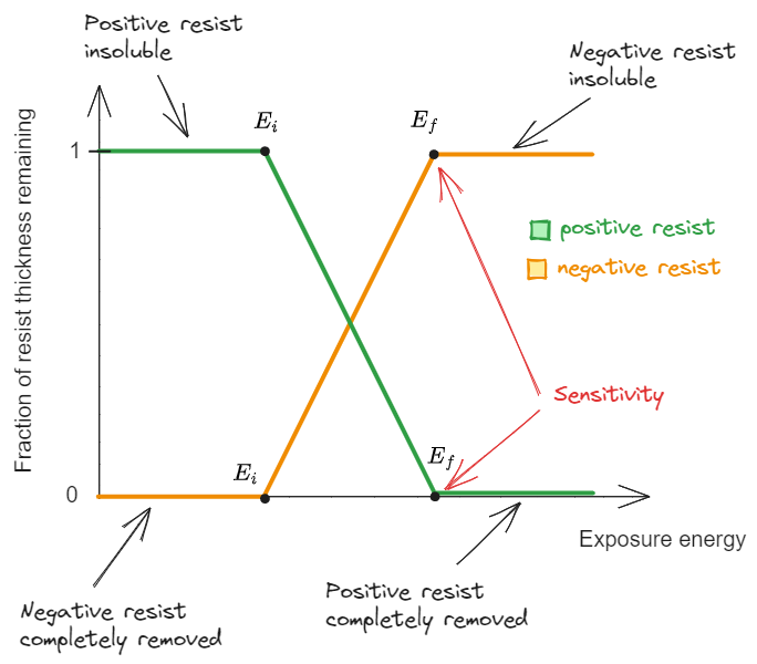
Polarity is the property that defines which part of the resists will become more soluble and which less soluble after exposure.
In a positive resist light breaks the polymer chains making them more soluble, this will replicate the same pattern of the mask on the resist. In a negative resist, on the other hand, light makes the polymer chains less soluble by inducing cross-linking, a negative resist will remain on the wafer in the places where there were holes in the mask.
There is also a third kind of photo resist called image reversal, which will be described in a following section.
Positive vs Negative
- Positive: light creates holes
- Negative: shadow creates holes
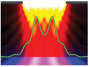
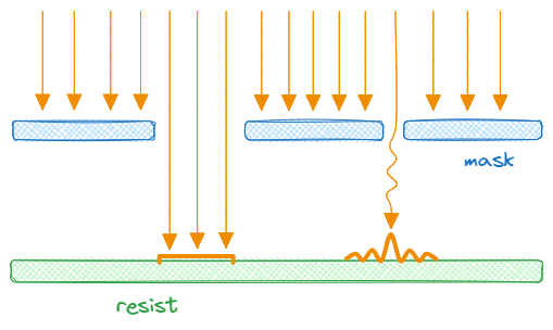
In the image below we can see that the light intensity is higher in the middle, thus the exposed region will have a “V” shape.
Resolution
Resolution capability is the smallest opening or space that can be produced in a photoresist layer and is related not only to the resist itself but also to the processes. Usually a thinner layer will have a better resolution while a thicker one will be stronger to mechanical or chemical stresses. Positive resist has a better resolution due to the smaller size of polymer.
Sensitivity
Sensitivity is the minimum energy density required to get the full transformation of the resist: the more sensitive, the less energy is required.
Contrast
Contrast is defined as the maximum slope of the development rate curve; it depends on the resist but also on the process, wavelength of exposure, etc.
High contrast ratio means “vertical” walls which most of the time means good quality. For cost or practical reasons sometimes lower contrast might be preferred.
Mask generation
Masks are fabricated with a lithographic technique which is highly accurate but extremely slow (and thus wouldn’t be possible to use it for manufacturing). A transparent substrate (quartz or soda lime glass) is covered with a
In addition to the real design, it is important to add alignment marks to the mask to allow precise positioning during manufacturing (where multiple masks have to be used to build a single part). These marks are typically crosses placed in the same spots which will later be overlapped to guarantee a correct placement.
Priming
Before starting the preparation of the wafer, it need to be dehydrated in a convection oven to remove water that it absorbed while stocked. After that a primer can be applied to improve adhesion of the resist in the next step.
Resist coating
Since most of the resists are liquid they can be applied by placing a small quantity on the wafer and spinning it to distribute the resist on the surface. The spinning speed has to be controlled in order to achieve the desired resist thickness. Usually the wafer is spun slowly at first to spread the resist and than the speed is increased to refine the surface and the thickness.
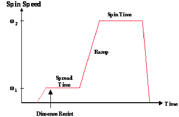
Due to surface tension there may be an accumulation of resist on the edges (called edgebead) which can decrease the usable surface area of the wafer.
Resist soft bake
At this stage the resist is still liquid and thus cannot be handled. To solve this issue wafers are heated to let the solvent evaporate. The temperature and baking time have to be controlled accurately to prevent damage to the resist (which may crack if heated too rapidly) and to obtain the proper result.
Resist exposure
Exposure is the process of providing energy to the resist in the spots selected by the mask. The energy source can be a lamp, a laser or an electron beam. It is important to note that the lower the wavelength of the light source, the better will be the results: light passing through an aperture of width similar to its wavelength will form a diffraction pattern.
Process flow
Exposure sources
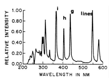
Mercury vapor lamp
The most common source is the mercury (
Nowadays there are also LED lamps that mimic the effects of
Deep Ultra Violet (DUV) laser
Since a lower wavelength means higher precision, there are more expensive alternatives to the
In this type of laser, a gas made of two (for example Kripton and Fluorine) is exposed to high intensity energy to make the two elements react and “bind” together. When the excitation energy is removed, the excimer dissociates and releases the energy at the characteristic wavelength. A pulsed excitation is used to repeat the process.
Extreme Ultra Violet (EUV) lasers
An even more advanced kind of lasers allows to reach wavelengths of around 13nm but is extremely expensive. The laser beam is produced by hitting a droplet of molten tin twice with a laser; the second time the droplet is hit it creates plasma that emits the desired wavelength.
Since EUV is absorbed by everything, this technology has to operate in vacuum and has to use reflective optics and reflective masks.
Electron beam
This technology uses a focused beam of electrons instead of light to expose a radiation-sensitive resists. In this way it is simple to obtain nm-scale features without the use of a mask (direct writing). Despite being accurate, this process is extremely slow since the features on the wafer are not exposed simultaneously.
One common type of resists used with electron beam lithography is PMMA.
Exposure techniques
There are different ways to expose the resist, each with pros and cons, here we will see the most common. It is important to keep in mind that the resolution can vary a lot depending on the exposure tool. The number that “defines” the resolution is the min line/gap period (
where
Contact
In contact printing the mask is applied directly to the resist; this method has the advantage of being easy to perform, cheap and fast. At the same time though, since the mask and the wafer come into contact, they can wear and get contaminated.
Another disadvantage is that the mask needs to have the same size of the wafer (large and expensive) since there is no magnification.
Contact printing is capable of high resolution but has unacceptable defects densities.
Proximity
This setup is similar to the previous one but in this case the mask is slightly separated from the resist, this reduces the resolution and increases costs and complexity but, on the other hand, there is no wear or contamination.
Projection
In projection exposure the mask is positioned very far from the wafer (~ 1m) and a set of lenses is used to minimize diffraction by performing a inverse Fourier transform. This method is extremely expensive and complex but have the following advantages over the previous ones:
- No mask wear
- Can introduce a demagnification factor (around 4x) which means that the mask can be cheaper.
- Higher resolution because only a small part of the mask is imaged
Because of the demagnification it is not possible to expose the whole wafer all at once though. There are two possible solutions to this problem.
- Projection stepper: in this method the wafer is translated each time a new die (a portion of the image, usually one chip) has to be exposed. Thanks to the use of precision stepper motors, the alignment of the mask needs to be done only once. For every new exposure it is important to set the correct focal plane to take into account wafer defects.
- Projection scanner: in this method both the wafer and the mask move (in opposite directions) to expose a single die. The die is not exposed all at once but is scanned, exposing only a small area at a time. This makes it possible to fabricate lenses that can be both smaller and less precise (since only a small part of the lens is used).
Alignment and exposure tools
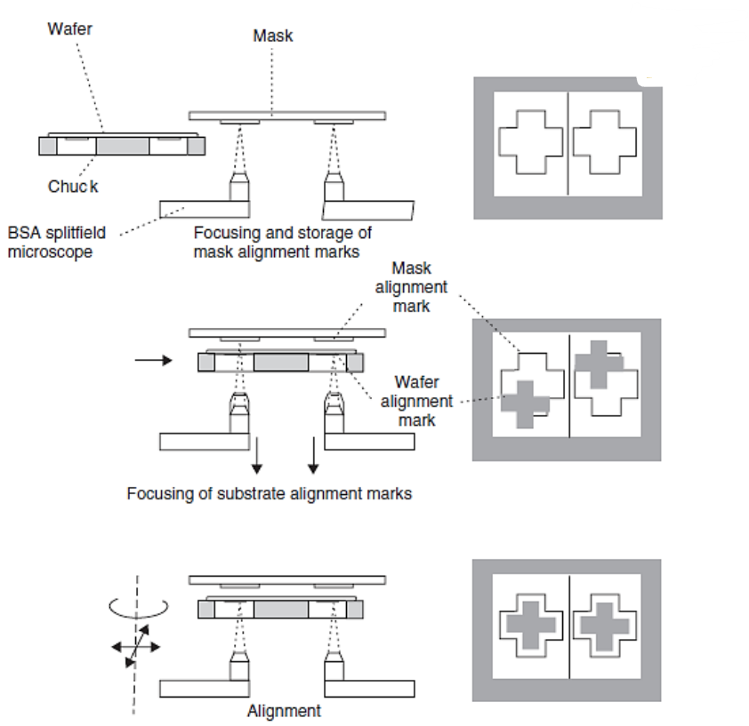
There are cases where it is necessary to align features on opposite side of the wafer. There are two main ways to perform this based on the properties of the sample: if the sample is transparent to some wavelengths (usually infrared), the samples can be aligned “normally” since it is possible to see the alignment marks through the sample itself.
On the other hand, if the sample is not transparent, a more complex method is required. In this method the mask is inspected from underneath with a microscope to identify the alignment marks and their position is stored. Afterwards the wafer is introduced in the machine and aligned according to the stored marks.
Reflections and standing waves
When exposing the photoresist, the light can be reflected by the surface of the wafer and interference patterns can form between the incident and reflected beams. This causes an intensity variation across the thickness of the resist, causing inconsistent exposure and thus inconsistent features.
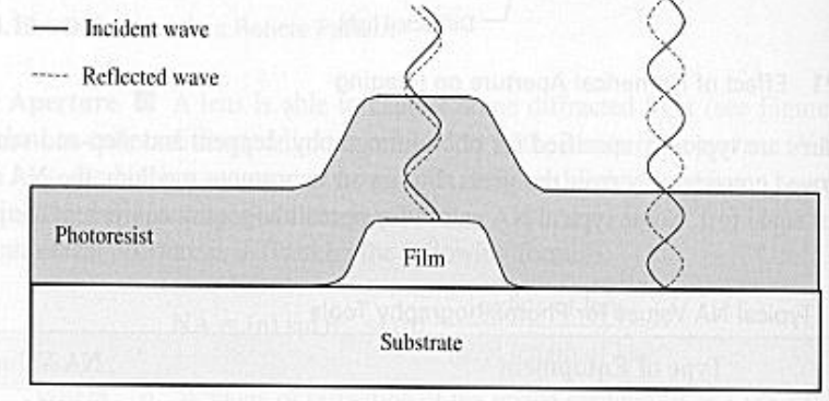
One possible solution for this issue is to coat the wafer with an anti reflecting coating before spinning the photoresist. This coating can reduce the issues but introduces more steps. Another solution to mitigate this issue is described in the next section.
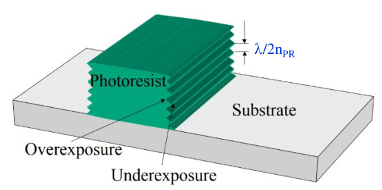
Resist post exposure bake
The resist post bake is an optional step that can help mitigate the effects of the standing waves seen previously. The bake facilitates the diffusion n the exposed and unexposed resist and thus smooths the waves.
The image below shows the effect of the post exposure bake.
It is important to notice that overbaking can reduce the contrast ratio.
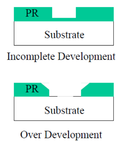
Resist image developing
The development dissolves the exposed/unexposed parts of the resist (depending on the type) and reveals the pattern.
There are two method to develop the wafer: immersion development consists in placing the wafer in a developer bath, in spray-on development, on the other hand, the developer is sprayed uniformly on the resist. In both methods the timing is critical: exposing for too long can worsen the results by removing unwanted resist, underexposing can cause even higher damage by preventing access to the substrate.
Resist hard bake
Hard baking is another optional step that can be performed to evaporate all solvents in the photoresist. This could be needed for wet etching or to make the resists harder and give it better implantation resistance, to improve the adhesion with the surface, or to reduce pinholes. Similarly to the post exposure bake, over baking the wafer can lead to decreased resolution.
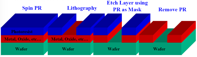
Etching vs Lift-off
Both etching and lift-off are processes used to form a pattern with a thin film (metal, oxide, etc.) over a wafer.
Etching
In etching, the film is first applied to the whole wafer, the required regions are selected with photo lithography and finally the exposed regions are etched to reveal the pattern.
Lift-off
In lift-off the, on the other hand, re regions where the film has to be deposited are selected with lithography, the film is applied everywhere and finally the resist is dissolved to remove the unwanted sections of the metal film.
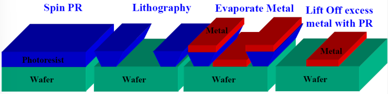
Benefits
The main benefit of lift-off is the fact that it doesn’t require an etchant for the metal. This becomes more relevant when the features that have to be formed are made of different metals; each of them would probably require a different etchant.

Problems
The main problem with lift-off is due to the fact that the contrast of the resist is not infinite and thus the metal film applied over it will form a continuous layer which can lead to peeling off unwanted regions.

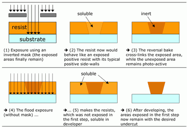
Image reversal
To solve the problem seen above, we could use a negative resists, that produces a negative slope, but as stated before negative resists tend to have worse resolution.
It is possible to use a special kind of photo resists called image reversal. The resist starts as a positive resist and is exposed using an inverted mask (the exposed areas are the ones that will remain). After being exposed, the resist is baked to make the exposed regions inert and the unexposed regions photosensitive. After this step a flood exposure is performed to make the non-inert regions soluble. After development, the parts of the resists that where originally exposed remain, but the slopes are negative to prevent the problems seen above with the lift-off.
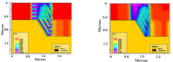
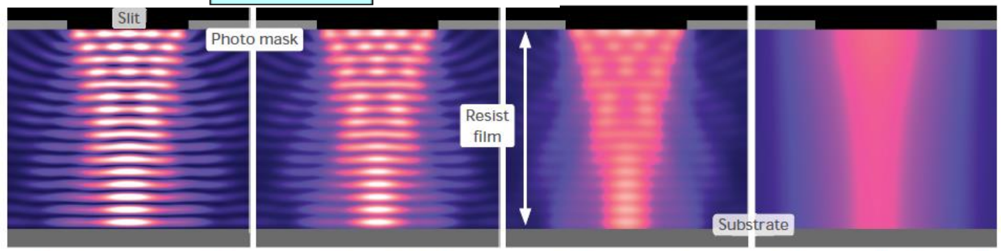
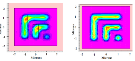
Models and simulation
Lithography simulations rely on both optics and chemistry, the first one to simulate the aerial image, the second to simulate the formation of the latent image in the resist.
The simulations provide a powerful tool to see in advance the effects of a change in the process (for example different wavelength, smaller feature size, etc.); the images below show how reducing the wavelength improves the results.
This other example shows how the post exposure bake reduces the effects of standing waves.