

Overview of the contents
Our goals are:
- find out how many charge carriers are present within the crystal
- where and how are they placed inside the crystal
- how do they move inside the crystal
to find out the answer to these questions we use models to help us approximate reality, of course like all models, these can only be used by making assumptions about their validity.
Free and independent electron model
The free-electron model, in solid-state physics, simplifies metals as containers filled with a gas composed of free electrons. These electrons are considered unbound to any particular atom and are able to move freely throughout the material.
Electrons in the model are:
- Independent: we can neglect interaction between electrons (Coulomb repulsion)
- Free: we assume that the potential inside the crystal is
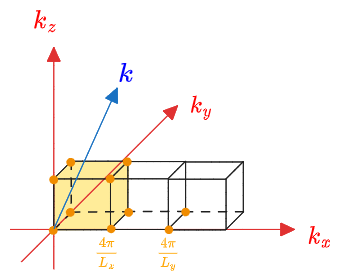
Let’s consider a crystal of macroscopic dimensions (

considering only one dimension at a time, this scenario is reminiscent of the infinity square well

We can then write the Schrödinger equation (SE)
for which we can write the general solution:
and the eigenvalues:
We want to study the properties of the material without worrying about the possibility of getting out of it (where the properties we are interested in no longer apply). So we apply an approximation by imagining that the lattice of the crystal continues to infinity. What we do is saying that instead of going “outside” the crystal, we enter in an identical one (i.e. we imagine being in a periodic matrix of crystals one next to the other).
This is called periodic boundary condition (PBC) or Born Von Karman condition and can be written as follows:
Applying
where
Since
We also know the following
The objective is to determine the quantity of charge carriers within a crystal.
Instead of directly counting them, we know that each charge carrier occupies a state, so we can use this formula to derive the number of charge carriers:
where:
represents the total number of charge carriers in the crystal. denotes the density of states. corresponds to the Fermi-Dirac distribution for a given temperature
In essence, this formula calculates the number of charge carriers by summing up, over infinitesimally small energy intervals, the product of the density of states at a particular energy level and the probability that the corresponding states are occupied by electrons (charge carriers).
Let’s derive the components of this formula.
Density of states (DOS)
DOS describes how the energy levels created by the lattice structure are distributed; it is defined as follows:
Where
We can find
Since
From which we can obtain
In 3D the
Fermi-Dirac distribution
Fermi-Dirac distribution gives the probability of a given energy state of being occupied at a given temperature.

The Fermi-Dirac distribution relies on the assumption of a continuous spread of energy states. While in metals, the values of
Independent electrons model
This model improves the previous one by dropping the “free electrons” assumption. This implies that in this case the potential is periodic, generated by atoms arranged in the lattice fashion:

For a periodic potential, the SE is
Bloch theorem
Note
See also Bloch theorem
Bloch’s theorem states that solutions to the Schrödinger equation in a periodic potential can be expressed as plane waves modulated by periodic functions.
The equality above can also be written as
The usefulness of Bloch’s theorem is that it allows us to restrict the search for the solution of Schrödinger equation from the entire space to the space of periodic functions. That is, functions that were once described in the unit cell can be extended beyond it periodically.
Similarly to what we did before we need to find
Since
In order to satisfy
Since
Remembering the reciprocal lattice definition
and by rewriting
we can see that the only term that survives (because of the
Similarly for all the directions:
So, finally,
this resembles a

From the drawing we can see that along the
Property of the Bloch state
Solutions of the Schrödinger equation that differ only by a reciprocal vector are equivalent (they describe the same physical state)

Given the property above, we can say that, given
So the eigenvalues are periodic.

In the (example) drawing above the energy bands are represented only between
It is important to notice that, differently from the free and independent electron model here the energy does not go continuously from
Example
Let’s consider the case of a solid made out of cells with only 1 atom with 1 electron.
We want to see:
- if the material behaves as a metal, a semiconductor or an insulator.
- if its properties depend on the size.
todo improve drawing
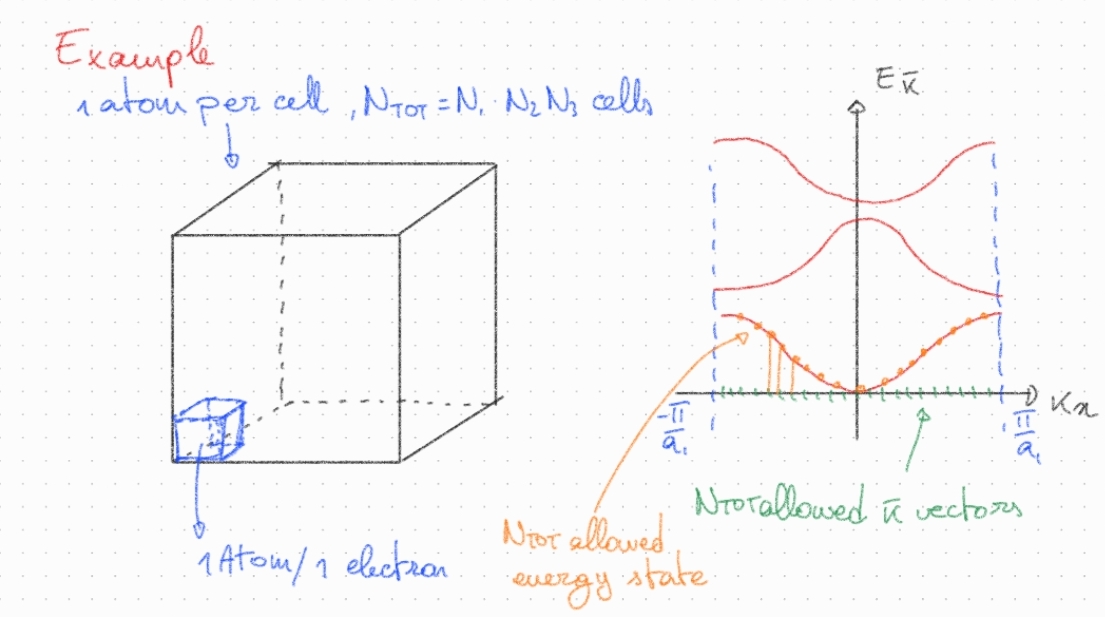
Notice that the red lines in the drawing are not continuous in reality for the reasons stated previously; this show that there are only
Considering that we have
If we were to double the size of the sample nothing would change since there would be
Effective mass
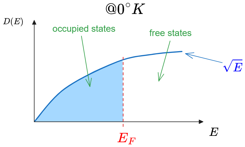
Recalling the definition of density of states, we can draw a very simplified plot of
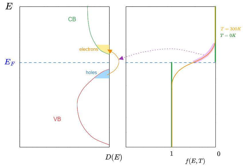
At
For temperatures above
Talking about the behaviour of electrons let’s try to analysing their mass, in the case of the free particle we have that the relation between mass, energy and momentum is straightforward:
but now we are inside the crystal and the relation is more complex.

at each
the motion of the electron can now be described by
It is important to notice that the effective mass depends on the curvature of the band, since the potential changes depending on the structure of the lattice.
The core electrons, the ones near the nucleus, have
The effective mass is a result of the interaction between the particle (like an electron) and its surroundings (the crystal lattice). In an anisotropic crystal (where properties differ along different axes), the effective mass can vary based on the direction in which the particle moves or interacts within the material. However, in an isotropic crystal, this mass remains the same regardless of the direction.
Effective mass and energy
The plots below show a representation of two energy bands (in blue) and the relative effective mass associated to them (in red).
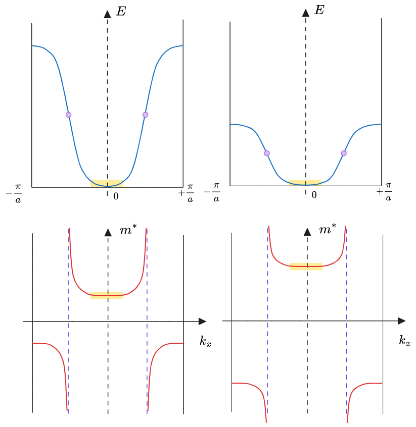
The yellow regions highlight the fact that where the band have a parabolic shape, the effective mass is constant (since it depends on the second derivative of the energy). In this region the mass can be calculate as always:
Where the energy has an inflection point the effective mass will tend to
Finally, we can notice that in the left plots the effective mass has lower absolute values since the second derivative of the energy is greater compared to the right plot.
Since electrons can have a negative effective mass, it is possible to consider them as fictitious particles with a positive mass and opposite charge called holes.
Parabolic band approximation
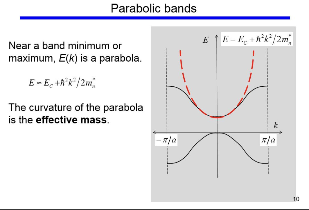
Near the maximum and minimum regions, the bands can be approximated with a parabola as long as we use the correct curvature for that parabola.
Substitutional impurities in semiconductors
Defects usually change the band structure generating new states in the energy gap, this is the case with doping (which is a substitutional impurity).

Example:
Substituting a 
If we calculate the energy