
Doping consists in introducing atoms in substitutional sites of a substrate to alter its physical, electrical and chemical properties. The doping levels can vary from
The most used atoms to dope
Doping silicon can change its conductivity by 8 orders of magnitude but can also alter its resistance to etching and its mechanical properties.
Methods
The two main methods for doping are diffusion and implantation.
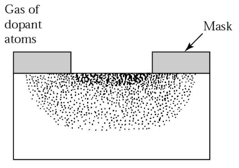
Diffusion works by exposing the (properly masked) substrate to a gas of dopant atoms which will diffuse inside the material with a pattern similar to the one in the picture. Due to the nature of this process, it is impossible to precisely control the size and shape of the doped region and, for this reason, diffusion is not used in nanotechnologies.
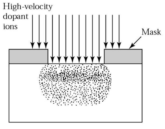
In implantation, on the other hand, the substrate is bombarded with dopant atoms which penetrate in the material. This allows for a better control of the amount of dopant and of the size of the doped region. The main disadvantage, which will be explained later, is that the dopant atoms, hitting the surface, damage the crystalline structure of the substrate, which has to be “healed”.
Doping parameters
To fully identify a doping process we need 3 parameters:
- Dopant distribution
or measured in - Total dose
measured in . - Junction depth
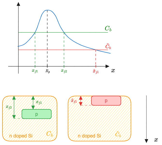
measure in or . The junction depth represent the intersection of with the background concentration . Considering for example a n-type doped substrate (see the CZ process), represents the depth at which the overall doping is neutral.

Ion implantation
Implantation consists in introducing desired atoms or impurities into the substrate in a controlled manner using a ionic beam.
A high voltage is used to accelerate the ionized dopants toward the substrate at sufficiently high speed and energies so that they can be implanted below the surface. (If the energy is too high we obtain the same effect of sputtering). Thanks to the way the process is performed, it is possible to achieve an instant on/instant off control; this, with the help of in situ monitoring, can allow for a better control of the implanted dose.
Implanter

The implanter is composed of multiple parts where the most important are highlighted in the picture. After the ions are emitted by the source, they are separated depending to their mass (A); this has both the advantage of filtering out unwanted species and allowing to select different dopants for different regions of the substrate.
After being accelerated, the beam passes through a beam trap/beam gate (B), which has the goal of filtering out those ions that got neutralized during the previous steps. This step is important for two reasons: the first one is that neutral atoms will not be deflected by the electric field of the scanners (C) and will end up bombarding unwanted spots; the second one, which will be more clear in the following, is that neutral dopants cannot be measured.
The scanners then move the beam to implant only the desired regions. The dose, finally, is measured with an integrator circuit (D) which measures a current which is proportional to the number of implanted ions according to the formula:
where
Gaussian approximation
Implantation can be studied as a random process which follows a Gaussian distribution: the more the dopant atoms penetrate into the substrate, the more random their path becomes. This can be represented in the following way:
 The plot has the depth on the horizontal axis and the concentration of dopant on the vertical axis. The depth at which the maximum concentration (peak concentration) is reached, is called range of implant or projected range and the “width” (or more properly the standard deviation) of the distribution around it is called vertical straggle. As we will see later, increasing the range of implant increases the vertical straggle.
Junction depth
Another important parameter of the implantation process, which is not shown in the plot above, is the junction depth, which is the depth at which the concentration of implanted dopant atoms equals the substrate background concentration of dopant atoms. It can be seen as the “line” between the n and the p parts.
If we vary the energy properly we can “sweep” the gaussian to obtain a mostly constant concentration.
Control parameters
When planning an implantation process, there are multiple factors that have to be taken into consideration to achieve the desired results:
- Ion energy: controls the depth and shape of the implant. Higher energies will make the dopants penetrate deeper into the substrate but will also increase the vertical straggle; this means that if we want to implant deeper (with a single implantation, more on that later) we will also loose accuracy. Increasing the energy has also the effect of damaging the crystal more (consider that the process is similar to sputtering).
- Dose: increasing the dose will, obviously, increase the concentration which, in turn, affects many device parameters, it’s mechanical, chemical and optical properties.
- Ion species: changing the type of dopant species has multiple effects. The most obvious one is changing the doping type (n or p), but the type of dopant affects also the profile depth and shape: some atoms (e.g.
) will have a higher projected range compared to others (e.g. ) at a given implantation energy. - Mask: the lithographic mask plays a very important role in implantation as we will see in more detail later. The main parameters of the mask that can be controlled are its shape, its thickness and its material. A thicker mask will be able to protect the substrate from doping.
- Annealing: changing the annealing time or technique has a major impact on the success of the process.
Annealing and activation
As stated before, when the atoms are implanted, they end up in random locations of the lattice but, for them to actually function as dopants, they need to be in substitutional positions. Moreover, the implantation process damages the crystalline structure, which has to be healed.
Both these problems can be solved with annealing, which consists in providing energy to the material to allow for the atoms to move in the “proper” places. This movement has also the side effect of causing diffusion of dopants and contaminants, which further reduces the resolution (the original Gaussian gets wider).
Isothermal annealing
In isothermal annealing the whole wafer is heated uniformly and slowly so that it never gets out of thermal equilibrium. There are two different methods of performing this type of annealing process:
- Furnace based: the wafers are introduced in a furnace where they are heated; the process takes a long time (minutes or hours) and for this reason there is a large redistribution of dopants.
- Rapid Thermal Annealing (RTA): in this case the wafers are heated by lamps and the heating process is dominated by electromagnetic radiation. The process is faster (seconds or minutes) and there is a smaller redistribution of charges.
Adiabatic annealing
In adiabatic annealing the thermal equilibrium is not maintained because the wafers are heated with a high energy density in a small spot. We have two types of adiabatic annealing: e-beam and laser. In both cases the heat transfer is caused by radiation and lasts for a very short amount of time (milliseconds or seconds).
Notice that, even though the heating time is much smaller compared to the isothermal annealing, this does not imply that the process is faster. In this case in fact, only a small portion of the wafer is heated at any given time, so the process has be repeated for each spot that has to be annealed.

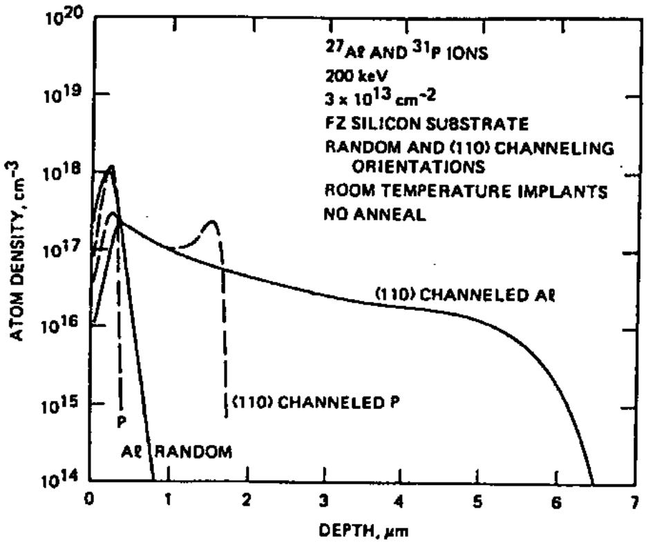
Channelling through lattice
In a monocrystalline material there is a significant probability that the implanted ions trajectory is aligned with crystallographic planes of low Miller indices (which are the most used); this causes the dopants to move in unexpected ways. If the atom enters in a channel, it will encounter less “resistance” and thus travel deeper into the substrate.
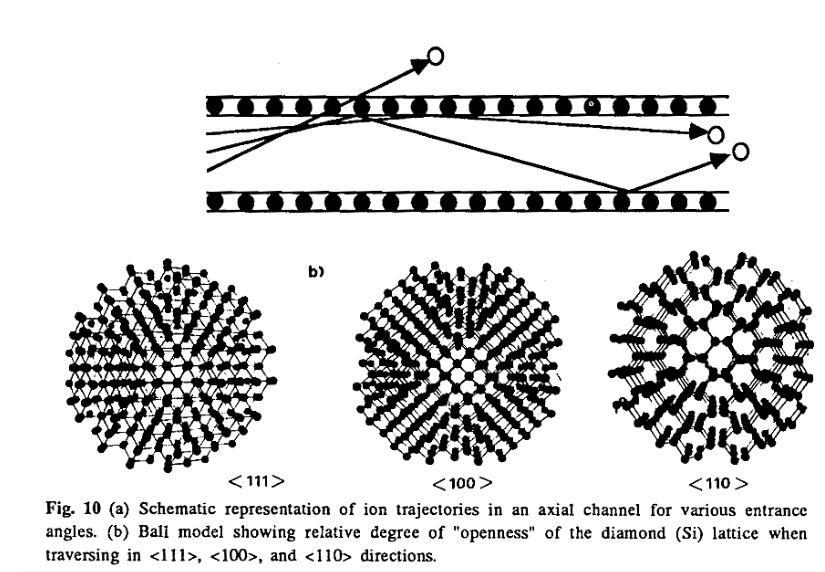
In the plot below we can see that channelling affects different dopant species in different ways but, nevertheless, its effect is very strong.
To mitigate the effect of channelling there are three possible solutions, each with its advantages and drawbacks:
- Implant into a damaged target: the surface of the target can be damaged before the implantation process by bombarding it with
and make it more amorphous. - Implant through an amorphous layer: similarly to the previous method, we could implant through a layer of
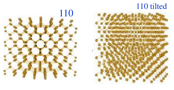
. This obviously requires two additional steps (deposition and removal of the oxide). This method has also the disadvantages of being only partially effective and difficult to implement. - Implant not aligned with the channel: it is possible to angle the substrate compared to the implantation direction in order to reduce the effects of channelling. As visible in the picture below, a (110) crystal, tilted by few degrees, appears completely different.
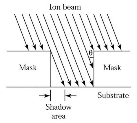
 Tilting the substrate has the advantage of being very easy and cheap but shadowing effects has to be considered.
Sheet resistance
Implantation through a mask
As briefly discussed previously, the usage of a mask offers a big range of control over the implantation. Apart from simply protecting the masked regions in a binary way, masks can be used to move the range of implant even outside the wafer itself.
This is possible because part of the dopants will remain in the mask; the thicker the mask, the less dopant will reach the substrate. The dopant distribution will have the usual shape but it will be spread across the interface between the mask and the substrate.
![]()
To calculate the part of dopant that reaches the substrate (the fraction transmitted
Where
The formula can be rewritten in terms of the complementary error function
Where
todo role of mask on FT
todo screen oxides (why oxides and not lito mask?)
Silicon on insulators (SOI) wafers
SOI wafers are a special type of wafers made to solve the problem of parasitic transistors in certain devices. What happens with classic wafers is that parts of devices can act as “unwanted” transistors and deteriorate the performance of the device itself. To solve this issue there is a special kind of wafer which has an oxide layer buried under the silicon device layer (the topmost part of the wafer).
The oxide create an electrical separation between the two
There are multiple ways of fabricating SOI wafers.
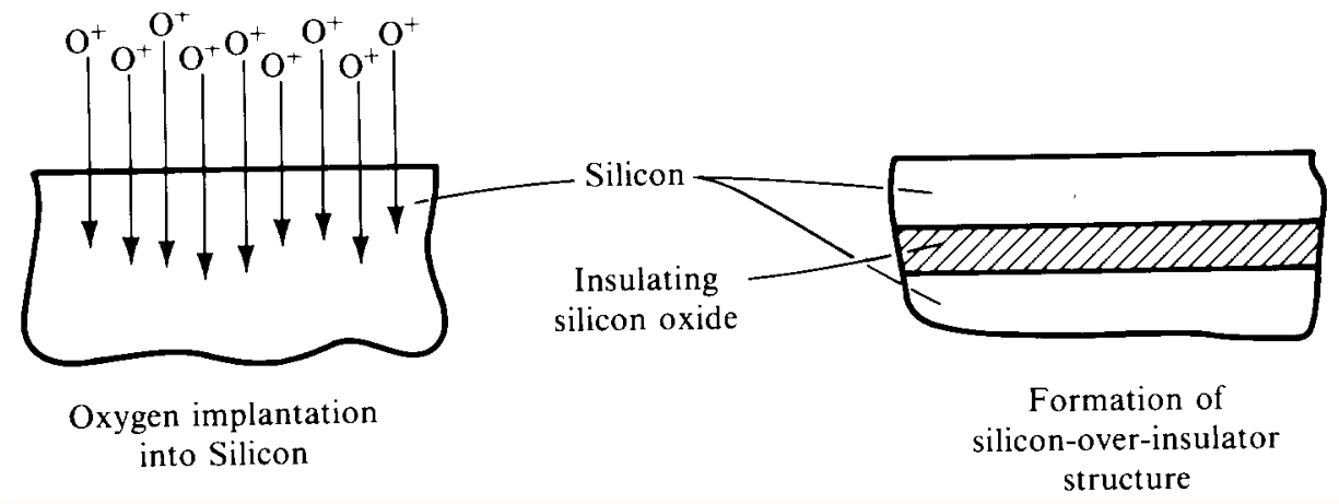
SIMOX
Simox stands for “Separation by IMplantation of OXygen”. The process consists in implanting oxygen ions in a normal wafer in order to oxidize a buried layer.
BESOI
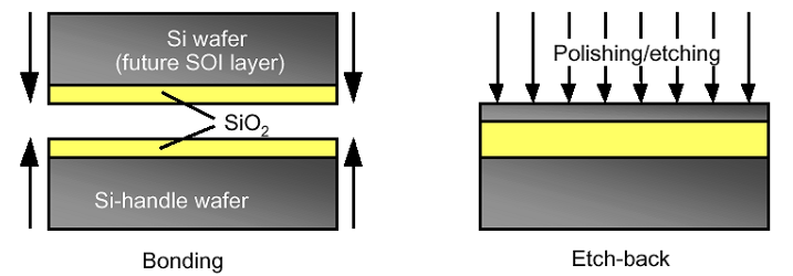
This method is based on wafer bonding and thinning, the name stands for “Bond and Etchback Silicon On Insulator”. In this technique, two wafers with an oxide layer on the surface are bonded together. After bonding, most of the top wafer is polished away, leaving a structure with a thin top silicon layer, a buried oxide and a full wafer below.
Smart Cut
Smart Cut is a variation of the BESOI process where the top wafer is “cut” instead of being polished away.
The “cut” is performed by pre-implanting the top wafer with
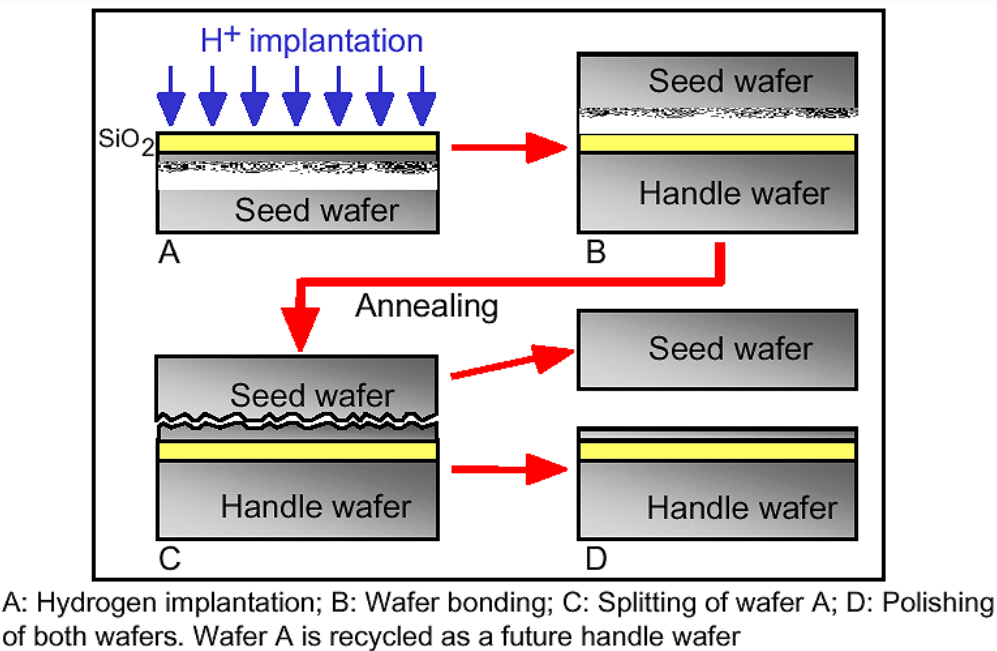
Finally a CMP polish is used to finish the SOI surface.
The process provides optimal usage of valuable material by placing the amount of materials needed for electronic functionality on top of a very inexpensive support layer.