
In physical vapour deposition a film is grown on the substrate by the condensation of a vapor.
Compared to CVD, where there was a chemical bonding of the film to the substrate, in PVD there is only a physical bonding: the material “sticks” to the cold surface.
Thermal evaporation
Thermal evaporation allows to deposit a limited amount of material (mostly metals). The process happens in a vacuum chamber where the material to be deposited is evaporated. The high vacuum allows to increase the mean free path, which is the distance travelled by the molecules of the gas before colliding with another molecule. A high mean free path is important because it allows the molecules to propagate in a straight line.
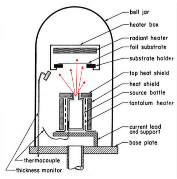
The vacuum chamber hosts the wafer (which is held upside down to reduce particulates) and a hot crucible that holds the material. The crucible is sealed by a shutter that can be controlled to achieve the right thickness.
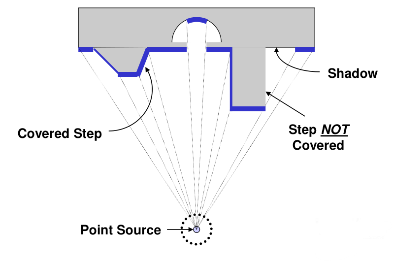
Since the vapour travels mostly in straight lines and the wafer is cold (no surface migration), the results are highly unconformal.
Crucible selection
Since the crucible is in direct contact with the material, it is important to select a crucible that will not react with it. Moreover, the crucible has to be conductive since it is heated by Joule effect; the most common choices are
If it not possible to find a suitable material, there are crucibles made from non conductive refractive material (ceramics) that contain a metal wire that heats up.
Advantages and disadvantages
Thermal evaporation has an high deposition rate (higher than sputtering) but it is important to choose the right crucible for the job. Also, not every material can be evaporated:
E-beam evaporation
In e-beam evaporation a conductive filament is heated up to electron emission. Electrons are then accelerated and deviated with a magnetic field to hit the material placed in a crucible (called liner). Since the liner is water cooled, there is no risk of contamination and the magnetic deviation separates the electrons from possible contaminants.
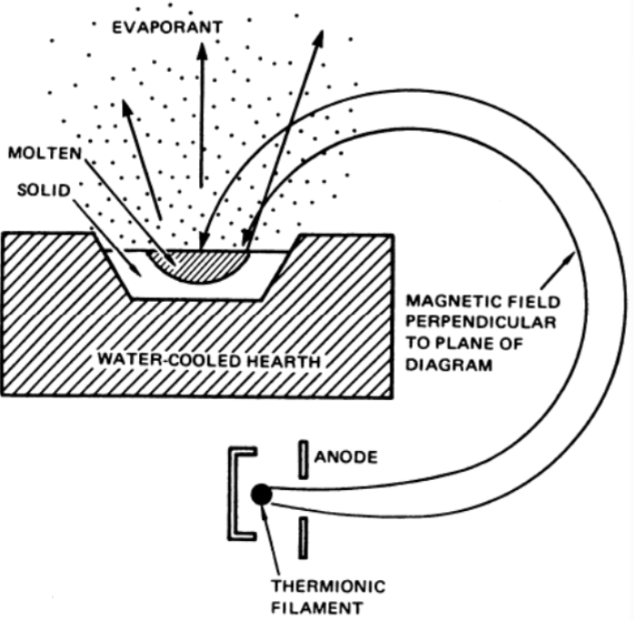
In industrial setups, one chamber can contain multiple liners, allowing for multiple evaporations without breaking the vacuum. This is extremely important not only for speed, but also to prevent material from oxidizing when they come in contact with air.
Being able to deposit multiple material one after the other can be helpful to exploit the advantages of different materials: for example a gold layer can be used for passivation (protection) and an aluminium layer for good conductivity at a lower price.
Apart from being able to evaporate materials without needing to worry about the crucible material, the other advantage of e-beam evaporation is that the liners can host a great amount of material and thus thick films can be deposited in one step.
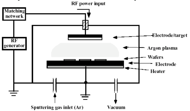
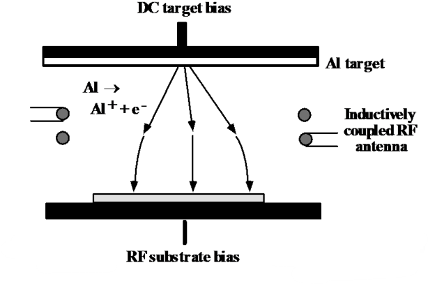
Sputtering
Sputtering is a technique that consists in bombarding the material we want to deposit (the target) with ions or atoms with high kinetic energy (usually
The advantage of sputtering is that the it has no limitations on the materials that can be deposited but it is more expensive compared to the previous techniques and can cause more contamination.
Similarly to PECVD there are two variations of sputtering based on the type of voltage used.
DC sputtering
In DC sputtering the substrate is placed at the positive potential and the target (the material to be eroded) at the negative. Several hundred volts are applied in order to form a plasma which accelerates the Argon ions. The ions hit the target and dislodge its atoms which fly off and stick to the substrate.
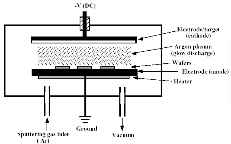
The main limitation of DC sputtering is that only conductive materials can be deposited. This is due to the fact that, if we use a non conductive target, positive charges due to ions would build up on the target’s surface, creating an opposing potential that would stop the reaction after a short period.
RF sputtering
RF sputtering solves the issue with dielectric material described above since it prevents the build up of charges on the surface of the target. It also has the side effect of not affecting the ions, whose mass is too high to be affected by fast frequencies.
As a side effect, the process is 50% slower compared to DC sputtering, since the bombarding occurs only when the ions move towards the target.
todo ??? above
Conformality and step coverage
Compared to evaporation, sputtering is more conformal since the source of the material is wider (in evaporation it was point like). This makes the particles arrive at the substrate with different angles so that they can “fill” even tighter areas.
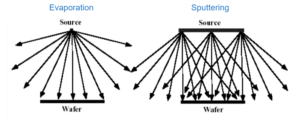
Since the substrate is kept cold, the atoms that hit its surface stick immediately and there is no surface migration. This causes the top faces to grow faster, making the issue even worse.
Magnetron sputtering
Magnetron sputtering aims at improving performances of the two previous methods increasing the ionization degree of the atoms in the plasma. By increasing the ionization degree (the number of atoms ionized) it is in fact possible do deposit more material at a given pressure. This also means that it is possible to maintain the deposition time constant decreasing the pressure (and thus reducing contamination).
The goal is achieved by introducing a magnetic field perpendicular to the electric field in order to put the electrons in a helical orbit. Since the new orbit will be longer, the electrons will have more chances of hitting an atom and ionizing it.
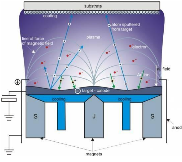
The main disadvantage of this method is that the target is eroded non uniformly (due to the circular paths of the electrons); this can make part of the material unusable (unless “recycled”), increasing the costs.
Reactive sputtering
Reactive sputtering is a technique that can be used both for depositing dielectric materials and for adjusting the stoichiometry of the deposited material.
The mechanism is similar to DC sputtering but, in this case, the gas that forms the plasma is reactive and will be incorporated in the newly deposited film.
For example, if we want to deposit
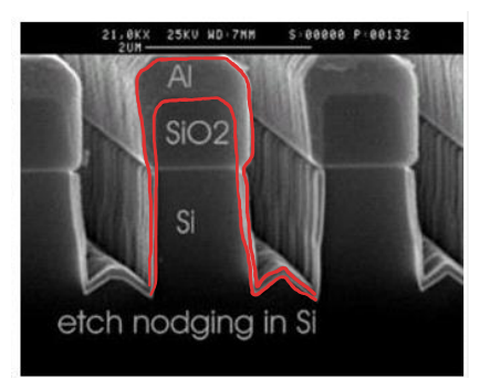
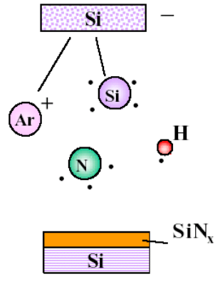
Ionized sputtering / HDP sputtering
Ionized sputtering aims at creating a highly non conformal layer. This is done by ionizing the atoms to be deposited so that they follow vertical paths, arriving at the substrate with a minimal deviation.
todo A typical application of this method is depositing material at the bottom of trenches. For example when creating vias it is important to place a thin
Electroplating
Electroplating is the oldest deposition technology due to the simplicity of the apparatus.
The simplest form uses:
- A bath consisting of an electrolyte containing metal-ions
- An electrode or substrate on which the deposition is desired
- A counter electrode
- An external power supply
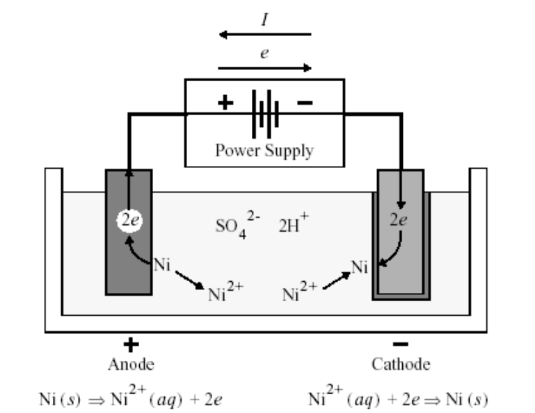
When a current flows through the electrolyte:
- cations move toward the cathode
- anions move towards the anode
- they may deposit on the electrodes after undergoing a charge transfer reaction (incorporation of metal into the solid)
todo Write better
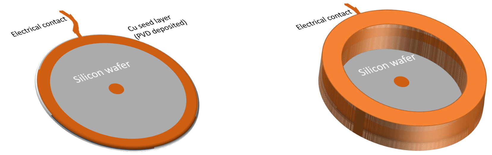
Before doing the procedure above, a conductive seed layer has to be created for the process to occur. This layer can be deposited with another technique (e.g. lithography + PVD). As well as being conductive all the places that we want to electroplate need to be electrically connected to the electrical contact, otherwise the process will not happen.
Comparison with Epitaxy and CVD
| Epitaxy | CVD | PVD | |
|---|---|---|---|
| Bonding | Grown | Chemical | Physical |
| Precursor | Vapour, Liquid | Vapour | Solid |
| Types | VPE, LPE, MBE | APCVD, LPCVD, PECVD (AC, CD), ALD | Thermal Evaporation, E-beam evaporation, Sputtering (AC, DC, Magnetron, Reactive, Ionized) |
| Metals | No | Yes | Yes, but not all of them with T.E. |
| Semiconductors | Only if they have similar crystalline structure and lattice parameter | Yes | Yes, but not with DC sputtering |
| Oxide | Only if crystalline (maybe) | Yes | Same as semiconductors |
| Conformality | Medium- High | Medium, Highest for ALD | Low for evaporations (point like source), Medium for sputtering, Non conformal for ionized sputtering |
| Temperature of wafer | High | Medium, Lower for PECVD | Low |
General comparison
This is a big comparison of some topics that I found confusing. (right click on the image and select “Open image in a new tab” to enlarge it).
